PRINTED CIRCUIT TECHNOLOGY
Francisco Jesús Lázaro Lorente
Content
1. Introduction to PCT.
2. Practical works - Laboratory.
3. Integrated Project.
4. Conclusions.
5. Future improvement.
1. Introduction to PCT.
Printed Circuit Techology PTC is an elective subject taught by Andrés Roldán Aranda at the University of Granada for students in the fourth year of the Bachelor of Telecommunications. In this course, the student can move into this exciting world of manufacturing technology from the analysis to the pre-production unit of an electronic products, from its conception to the end of its life cycle.
2. Practical works - Laboratory.
In this section I will discuss the knowledge gained in the laboratory of this subject. In the laboratory sessions our goal has been to learn the different techniques for soldering components onto the PCB. The tools we have used are:
Hot Air Gun desoldering.Hot air guns is one of the tools used in the laboratory. This tool only is useful with surface mount technology packages (SMD). It can be used with Through-Hole components, but it is less effective. To use these guns must first configure the parameters of temperature and airflow. Once we have configured these parameters to the needs of our components we can proceed to desoldering. When desoldering must take into account the use of different nozzles according to the encesidades, hot air introduccir perpendicular component, use tongs to not burn.
Desoldering Gun
The desoldering gun is an specific tool to desolder Through Hole components. Gun head which is heated and when the correct temperature is brought into contact with the pins when the tin component is melted by pressing the trigger to absorb said tin. Therefore this technology is very accurate with Through-Hole components. In this type of technology must take special care in maintaining since the absorption of tin can obtruir ducts gun so every so long to open and clean.
Soldering Iron
The welder is the most basic welding when the tool components to a PCB. This instrument and what we had used in other subjects and is very useful for Through-Hole components but instead for SMD components is much more complicated. When working also have to adjust the temperature to the needs of even each component being soldering or desoldering, because if not it can burn the components.
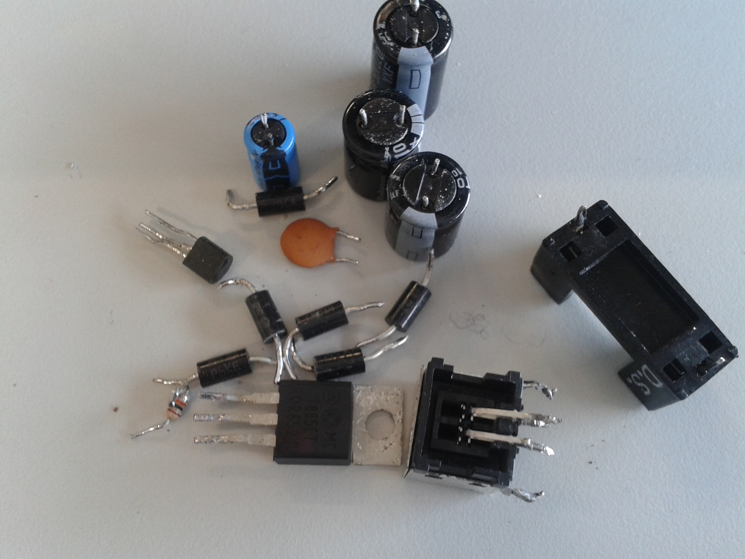
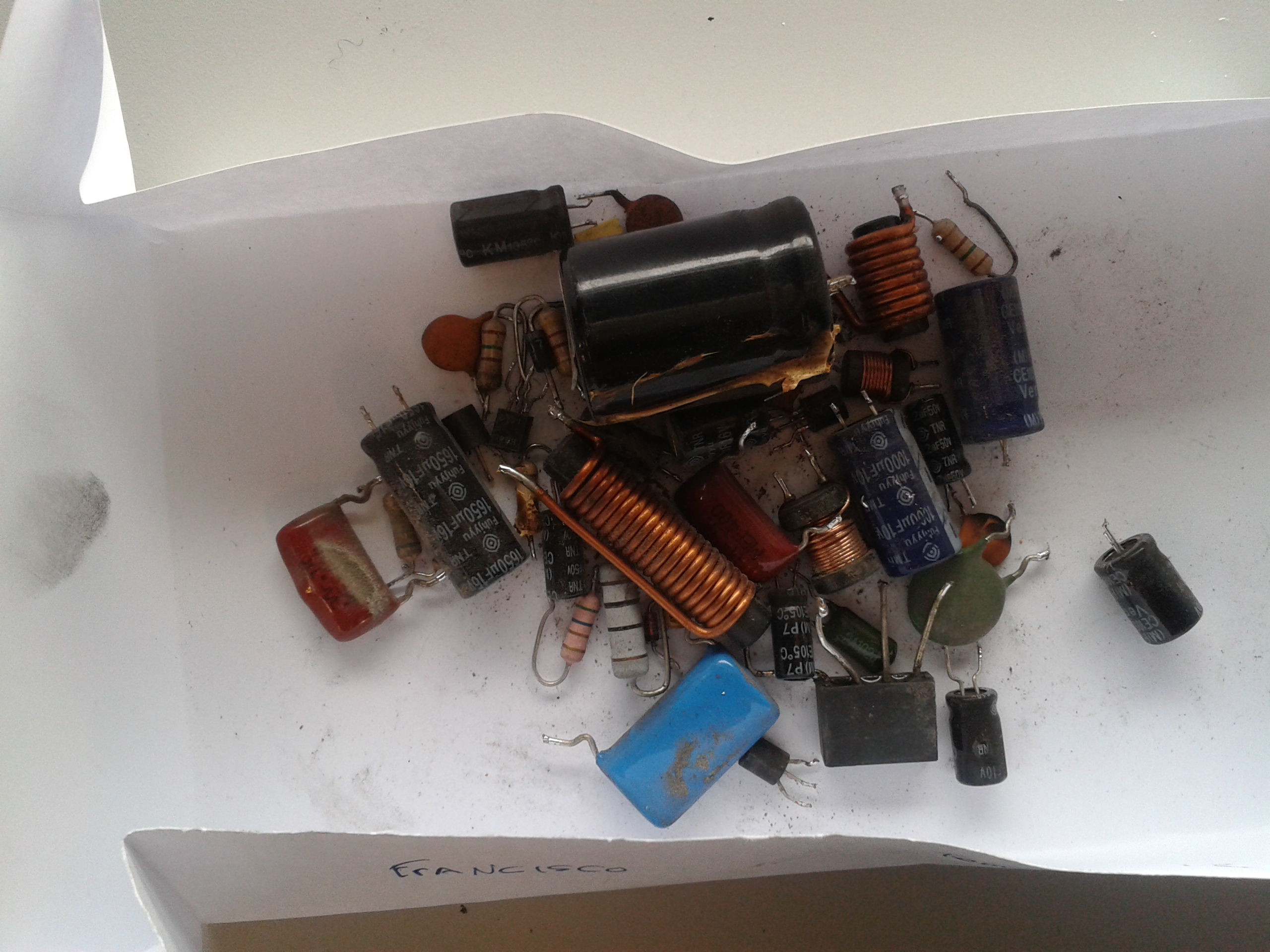
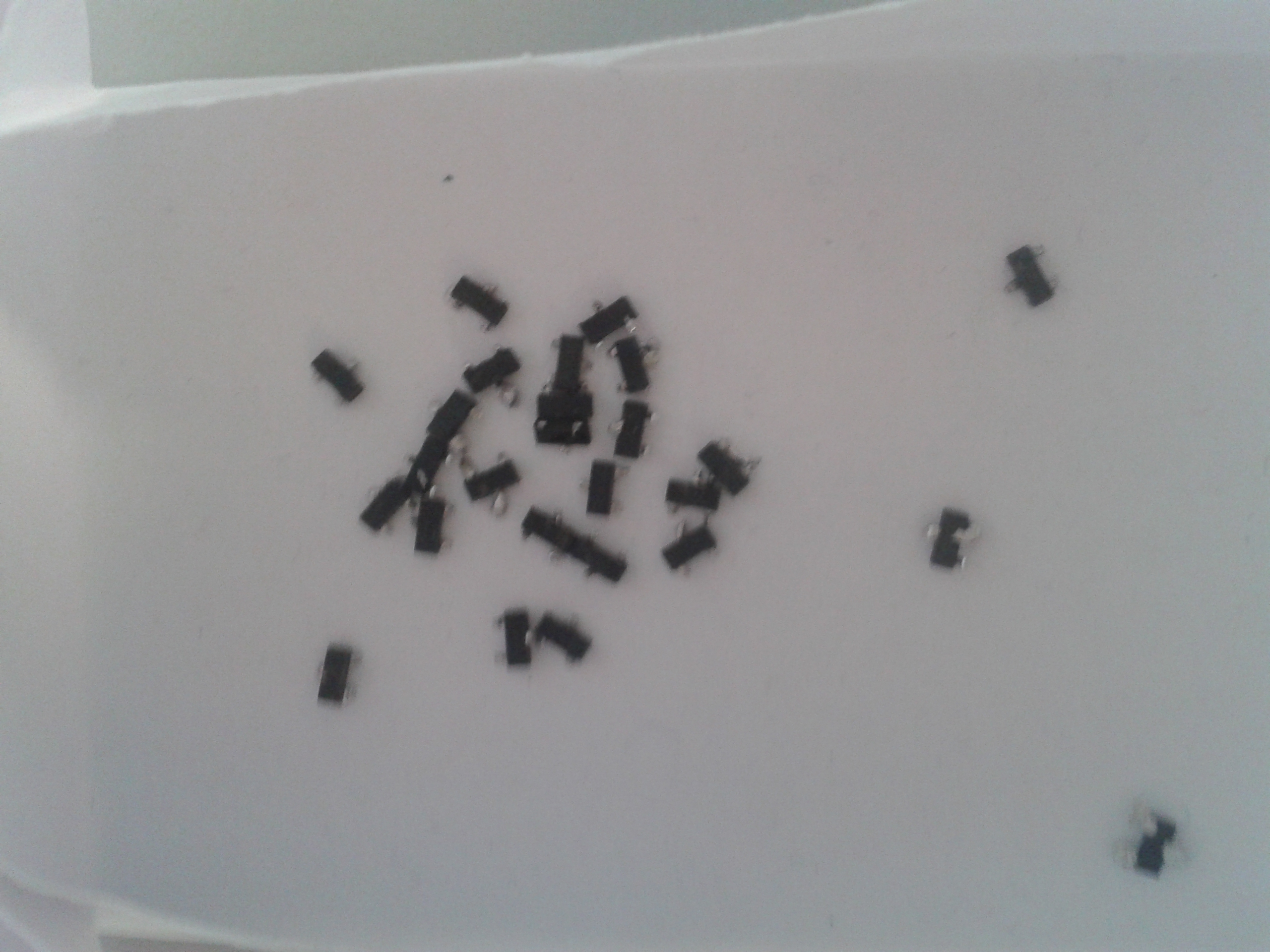
Finally, I will show some pictures where you can see the components I unsoldered along practice sessions of this course:


As we can see from the above two figures almost every component I unsoldered using the tools described above are of Through-Hole type and it applies a temperature more or less than 350 °C.
3. Integrated Project.
Apart from the practical sessions in this course we will carry out a small PCB project. In my case I decided to do a electronic dice (Dael). My project is based on another project I found on a website that you can see here or in the following videos:
The components that make my Dael are SMD resistors, capacitors (both electrolytic as ceramic), led diodes, transistors and finally we have 2 integrated
one that is a pulse controller (LM555) and the other is a 10-bit digital counter (74HC4017).
List:
First, we outline a circuit that meets our needs.
Next step, using the Altium program create libraries with Footprind and 3D models of components.
Once created these libraries, assemble and simulate the circuit in Altium to check its functionality and debug errors.
Moreover, when the circuit work correctly, the next step is the design for it has used the Solidworks program.
When we have reached this point I have to make a decision to compromise between design and mechanical eletrico to meet both mechanical as well as electrical needs.
Finally, assemble the two parts (mechanical and electrical part) and check that everything is correct.
ELECTRONIC DESIGN
Now I will talk about the electronic product, as I mentioned earlier, we will use the software to implement such Altium electronica, since this software also can create the PCB from the schematic.The schematic you can see here or on the image below:

The components that form this schematic I created also using the Altium, I had to create both the schematic component, such as footprint as the 3D model.
Below introduce links where you can download these files:
Once all components have already created and also we mounted our PCB schematic create and place their orders for components so that then can be coupled to the mechanical design. Below you can see a video of how it has been my PCB:
Also in the project we performed a section of paneling as you can see in the picture below:
In the above link you can download all files required for paneling (Gerbes files, NC drill, etc.)
Bill of materials:
MECHANICAL DESIGN
In this stage of the project we will focus on the physical aspect of the product for this we will use the Solidworks program. After several designs I opted for a cylindrical design, which will be divided into two parts (a base with lid).
Product Top:
Product Bottom:
Product with PCB:
So that the end product is:
The SolidWorks tool gives us the option of giving the values of volume, weight and center of mass of our product.These parameters can be seen in the image below:
In the following video we can see the assembly of all parties:
To implement the parts we use a 3D printer. The software uses this 3D printer is called "Cure". With this software we can see a simulation of how building practically the piece and other parameters such as the time duration and the amount of material used.
4. Conclusions.
In this project I have invested much time, since before the subject of Printed Circuit Technology had a complete lack of circuit fabrication technology.
It was not only about PCB design, but we have approached the actual design process that is followed with any product, from idea to prototype. Thanks to this,
we have achieved a vision of how things work during product development, being involved in all of them.
Learn the software used (Solidworks, Altium, ...) has been a task a little hard, but it's really gratifying to see that with effort and a little ingenuity,
we can design a product from scratch.
5. Future improvement.
As for the improvements that can be case may be enough since being my first project is not very sophisticated. think we can correct both in the electronic
design and the mechanical design.
In the electronic design I think it could have synthesized design using much more technologically advanced components to save on materials and space.
And for the mechanical part is where most deficit may have. I had to have found a more optimal design in terms of space. To say that one of the major problems
of my design was the large size of the battery and therefore Reducers serious battery one point to change in future upgrades.