RECORDAD:::::: EN ENGLISH
Tenéis libertad para meter/cambiar los apartados de este documento.
La idea es que contenga todos los resultados de vuestro trabajo en esta
asignatura.
Todos los contenidos deben
dar la posibilidad de descargar las fuentes del trabajo ya sean PDF, ZIP, piezas Solids.... para que sea útil para la comunidad de estudiantes.
Más recursos....
en la WEB del pasado curso.
Me tenéis que facilitar una
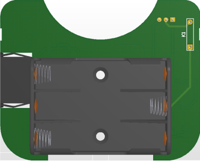
imagen para ponerla como resumen
de vuestro proyecto en la web con vuestros nombres.
Ledificador
Pedro Jesús García García
pedro2g@correo.ugr.es

First at all, before describe the
main integrated project, different activities made throughout the course will
be presented.
1.
Desoldering techniques
In some practical
courses, we have learned to desoldering electrical
components from real circuits. The components desoldered
were both Through-hole Technology (THT) and Surface Mount Technology (SMT) as
shown in next pictures. The process will be explained below.
·
THT:
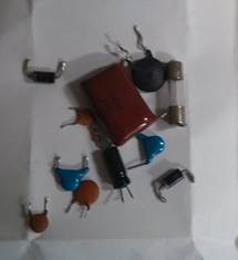
as we know, THT components pins go through all the PCB layers. In
previous years, THT components were desoldered
melting the tin with a soldering iron and removing molten tin with a desoldering pump. But this year a soldering/desoldering machine can be used, so components could be
easily desoldered with a Desoldering
Gun tool which, connected to the machine, can melt and suck away the melten tin. But sometimes, some component pins have no
enough tin or you have not sucked away all of it so we have to add more tin
with a soldering iron before can remove all the metal. For this process we have
used a temperature of 350ºC. In next picture we can observe some capacitors,
diodes and a resistor desoldered.
·
SMT:
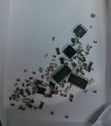
these components have their pins soldered on the surface of the
PCB, whether in the top layer or the bottom layer. This technology is new for
us thus we have learned to desolder it with the Hot
Air tool of the soldering/desoldering machine. With
this tool, a hot air flow is blown which we can heat the entire SMT component
and melt the metal under it. Therefore, with tin molten, we can remove the
component with tweezers. In the picture we can see a lot of components desoldered with a flow of 350ºC too and an air pressure of
85 P, like resistors, capacitors, diodes, arrays of resistors, and others SMT
packages (SOP).
2.
Copper Clad project
Falta por hacer!
3.
Integrated Project: Ledificador
3.1 Introduction
In this project, a
frontal bike light named Ledificador
will be developed. This light will be composed by high power LEDs, which are
more efficient and luminous than standard high power lights. With this, all the
knowledge acquired at Printed Circuit Technology course will be put into
practise.
3.2 Design flow
To explain the design flow, a graphic
diagram is going to be used.
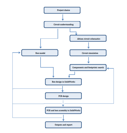
First, the project was
chosen searching among those in Elektor magazine. I
chose this one because of its complexity and because it was a product useful
for me since I don’t have a powerful bike light and it is interesting for me to
learn how to do it. The Ledificador was found July-August 2009 magazine.
Next, a circuit study
was made in order to understand what is going to be fabricated.
Once the circuit was
understood, two tasks were developed in parallel at same time: the box model
design and the schematics in Altium. The first phase
is very important in the product design since the PCB design (with all its component) depend on the box. To do the schematics,
the project schematics in Elektor magazine was used,
but a circuit simulation was made in order to can calculate the power that
components have to support, and can choose them properly.
So now, the box design
can be built into SolidWorks. Once built, improvements were added into the
design until the box is totally finished and we have then the final box
product.
With this, we are ready
to design and make the PCB. For this, the size of our box is used to describe
the boarder outline. In this step all the components chosen have to be placed a
connected, so if there are problems of space we can redesign the box or change
some components with others smaller.
When the PCB is well
designed, the assembly between PCB and the box is made. If everything fits
there is no problem, but if there is any inconvenient yet, we can redesign the
box model and start again.
Finally, the outputs
such as images, videos or profiles can be extracted, and the report can be
written.
3.3 Mechanical design
In this important step
of flow design, the box of our frontal bike light has to be conceived. We had
to consider a lot of constraints and problems such as:
-
technology of our 3D
printer
-
the way to place the
light on the bike
-
price
-
design attractive
-
the way to open the box
in order to change the batteries
-
the way to close the box
(and reopen) in order to assembly the PCB
-
components size
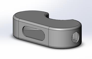
A first
basic model thought appears in above picture. One of the main
characteristics is its oval shape with the semi-circular form in the back. This
oval shape seemed to be attractive, but it wasted a lot of plastic in the sides
of the box, so a new basic shape was thought. With respect to the semi-circular
form in the back, it is thought to fit into the bike frame (based on my own
circular bike frame). For this, the way to hold together the light and the bike
is with an external not included trap, which passes into the box through two
holes located in the back size. This closing system will be maintained in all
mechanical designs. The right hole is thought for a generic ON/OFF switch and
the frontal one, for three power LEDs. The problem with this last hole is that dust can entry into the box, so other idea had to be
elaborated.
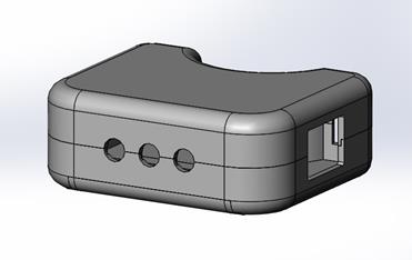
For this, a second and final model was
created. First, the model has now a rounded rectangular shape, in order to
reduce the plastic. In my opinion, this shape can be a little less attractive,
but it is made up for with the price reduction. The switch hole was changed to
fit the switch component chosen, and in order to avoid dust, three different
holes were opened for each power LED. For this reason, a slot was created in
frontal side to put in a small PCB containing the LEDs, as we can observe in
the pictures.
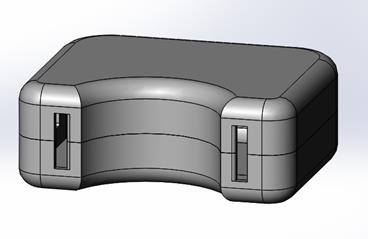
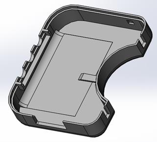
The box was divided by
the middle in two different parts in order to can introduce the PCB and the
battery holder. To close the box, a lips and hook
closing system was created. To change the batteries, a cover was made in the
down side with other lips and hook closing system. The size of the cover was
adapted to the battery holder. Finally, the way of maintain the PCB and battery
holder together and still was using the two holes of the battery holder: two
screw sink were built in the opposite side of the battery cover, so the PCB and
battery holder are fixed with two screws. With this, the box is finished.
A last problem happened
when battery holder didn’t fit into the box, so we have to make it bigger. This
was a flow design mistake since this problem should have been expected before
build the box.
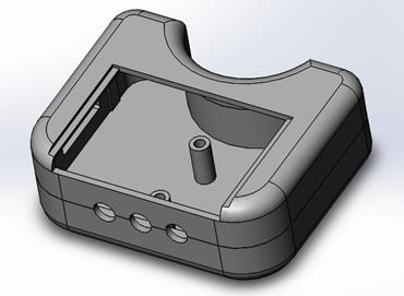
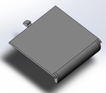
Some section pictures:
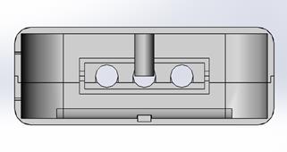
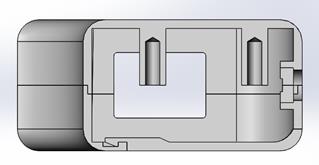
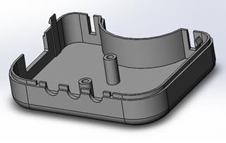
Next, we can observe the
views of the different parts of the box, with their dimensions.
Insertar vistas
3.4 Electrical design
Explicación del circuito, resultados
de simulación, enlaces a datasheets.
First at all, we are
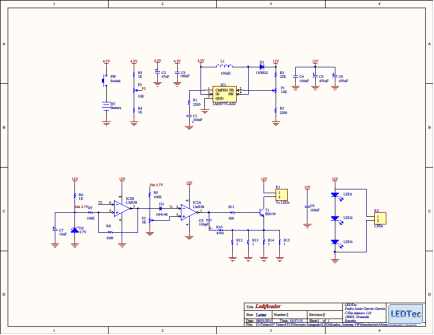
going to explain the circuit of the project chosen. The schematics appears in the image below.
The circuit has a 4.5V
source with a switch that feeds a DC-DC boost converter LM2577T-ADJ,
which supplies the rest of the circuit with 12V, necessary to feed the three power
LEDs. The IC2A is used as a current source for the LEDs, while the
second amplifier operational avoids the efficiency lost since disconnect the
circuit when the voltage supplied by the batteries are below 4V. Hence, the
LM2577 provides the necessary voltage and the LM358
the necessary current to the 1W LEDs. All these components were through-hole in
the original Elektor project, but we have chosen the SMT
ones when possible, in order to decrease the PCB surface needed.
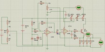
Normally, a complete
circuit simulation should have been carry out, but it was impossible to find
the LM2577T-ADJ PSpice model, so only a part circuit
simulation was made in order to choose the size of the SMT components properly
since, depending on the package size, the component may support more or less
power. The simulation was made in Proteus, where current and voltage in some
components were measured. In all components the power was less than 0.1W, so we
could use the 0603 package. If you click at the picture below, you can access
to the Proteus project.
3.5 PCB Design
Procedimiento seguido en
el diseño de la PCB y su relación con el diseño mecánico.
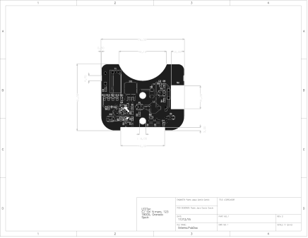
To do the PCB design,
the board
outline of the PCB was imported from the box of SolidWorks, with the
two holes for the screws, as we can see in the image below. After have the PCB
shape, the 3D components and their footprints were imported from schematics,
and were placed on the board in an organized way with the help of aligning
tools, using both top and bottom layers.
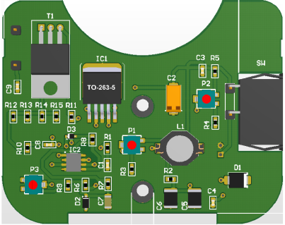
One inconvenient was the
placement of the switch, since the board outline imported from SolidWorks there
was not a hole for it. For this reason, a board cutout
was defined for the switch. Also, some 3D components had to be changed, as the
BD139 transistor in order to get a lied down component.
After that, the routing
was made with the Auto Route tool of Altium that
place the routes and the vias automatically.
However, the PCB was not
finished, because there was a lot of free copper space wasted, copper that had
to be etched. Because of this, in the second version of our PCB, a ground plane
was placed on the top layer. This way, there is no need to have a ground route
throughout the PCB, the ground is more stable and the etch copper is minimum.
With all this, the final
PCB can be observed in the pictures and video
below.
INSERTAR VIDEO!
3.6 Assembly of PCB and box
Finally, the PCB can be
exported from Altium to SolidWorks in a .step
file. In SolidWorks, an assembly
with the PCB and the box can be built and we can observe the final product in
the next videos.
INSERTAR VIDEOS!
3.7 BOM
Here
we can observe all the components of the project, some information and the
price. If you click in component name you can access to its schematics. Also,
the schematics Altium library with these components
can be found here
and the PCB library here.
|
Component |
Designator |
Supplier |
Unit price
(€) |
Amount |
Description |
|
R12, R13, R14, R15 |
RS |
0,018 |
4 |
Resistor ±1%, 0,1W, 0603 |
|
|
R11 |
RS |
0,008 |
1 |
Resistor ±5%, 0,1W,
Carcasa 603 |
|
|
R4, R5, R6 |
RS |
0,008 |
3 |
Resistor ±1%, 0,1W,
Carcasa 603 |
|
|
R1,R3 |
RS |
0,007 |
2 |
Resistor ±1%, 0,1W, Carcasa 603 |
|
|
R10 |
RS |
0,007 |
1 |
Resistor ±5%, 0,1W,
Carcasa 603 |
|
|
R2 |
RS |
0,008 |
1 |
Resistor ±5%, 0,1W,
Carcasa 603 |
|
|
R7, R9 |
RS |
0,008 |
2 |
Resistor ±5%, 0,1W,
Carcasa 603 |
|
|
R8 |
RS |
0,011 |
1 |
Resistor ±1%, 0,1W,
Carcasa 603 |
|
|
P3 |
RS |
0,288 |
1 |
Potentiometer ±25%, ±250ppm/°C, 0,1W,
SMD |
|
|
P1, P2 |
RS |
0,13 |
2 |
Potenciometer ±30%, ±500ppm/°C, 0,1W,
SMD |
|
|
D3 |
RS |
0,033 |
1 |
Diode 300mA, 75V, SOD-323 |
|
|
IC1 |
Mouser |
5,78 |
1 |
DC-DC boost
converter |
|
|
IC2 |
RS |
0,11 |
1 |
Dual Operational
Amplifier |
|
|
LED1, LED2, LED3 |
Farnell |
2,51 |
3 |
Power LED |
|
|
D2 |
RS |
0,028 |
1 |
Diode zener
2.7V, SOD-123, 2-Pines |
|
|
T1 |
RS |
0,246 |
1 |
Through hole
transistor |
|
|
D1 |
Farnell |
0,572 |
1 |
Diode smd,
DO-214AA |
|
|
C1 |
Mouser |
0,043 |
1 |
Capacitor 603 |
|
|
C3, C4, C9 |
Mouser |
0,052 |
3 |
Capacitor 603 |
|
|
C8 |
Mouser |
0,052 |
1 |
Capacitor 603 |
|
|
C2 |
Mouser |
0,363 |
1 |
Capacitor 2917, 16V |
|
|
C5, C6 |
RS |
0,055 |
2 |
Capacitor ±20%, 16 V |
|
|
C7 |
Mouser |
0,13 |
1 |
Capacitor 1206, 16V |
|
|
L1 |
Fastrongroup |
1,02 |
1 |
Inductor smd |
|
|
Total price = |
16,881 |
3.8 Conclusion
With this work we could approach
the actual process of PCB manufacture with all its design flow, from taking the
idea and requirements (this time from an electronics magazine), through the box
model, to the design of the PCB, including all feedback processes every time in
appeared a mistake or a problem.
Perhaps now, with the
project already implemented, if I started a new work, I would do things
differently, and some mistakes and subsequent modification by feedback could be
avoided.
Also, I think I have
managed to make a complicated project with many components and many decisions,
and surely other engineer with more experience could have made it in a better
way, but I am glad with the results.
3.9 Improvements
The project can be
improved in many ways, but only box and PCB improvements are going to be
mentioned, not electronics ones.
With respect to the box,
if the 3D printer allows, another system gripping could have been done instead
of a not included trap. Current bike lights have two different parts: the first
one is to grip to the bike frame, and the second one is the light itself, that
is assembled to the gripper. Also, another improvement, besides the shape, can
be adding a slot to the batteries cover for easy opening.
With respect to the PCB,
perhaps a better location of the components could have been done in order to
reduce the number of vias, or a lied down package for
BD139 transistor could have been found in order to increase the thermal
dissipation and ground connection.
3.10 Valuation of the course
In this work, the
difficulty was not the electronics since the project was taken from an
electronics magazine, but the box and PCB design. We had to learn about design
software (SolidWorks) and PCB design software (Altium)
among others. We have learned the design flow of a PCB and that it is not a
sequential flow, but it has feedbacks in order to improve the characteristics
or solve an error.
In addition, as personal
opinion, I prefer courses like this since the student can implement all the
concepts learned during the course in a real project, which brings you to the
real world of engineering. And also, as the course is in English, we could
practise the main language used in engineering, which prepares us for our
future.
