Report about the course of Printed Circuit Technology
Pedro
M. Vallejo Muñoz

Index
1. Introduction
2. Laboratory
3. Examination and recognition of the elements of a PCB
4. Main project
5. Copper-clad project
This course belongs to the last year of the Bachelor's Degree in Telecommunications Technology
Engineering (Branch of Electronics
Systems) of the University of Granada. Here ,
you can see the contents of the course.
The main goal of this report is describe the knowledge
and the skills developed during the course of Printed Circuit Technology
teached by Mr. Andrés Roldán Aranda.
In
this chapter you can see some videos token in the laboratory soldering some
components. We use this solder station to solder and disolder components.
2.1. SMD
SMD or
Sorface-mount technology is a technology in which the components are mounted
directly on the surface of PCBs. SMDs can be one-quarter to one-tenth the size
and weight, and one-half to one-quarter the cost of equivalent through-hole
parts.
2.1.1. SMD soldering
In
the following video you can see the process to solder a SMD resistor, capacitor
or similar components:
2.2. Through-hole
Through-hole
technology , also spelled "thru-hole", refers to the mounting
scheme used for electronic components that involves the use of leads on the
components that are inserted into holes drilled in printed circuit boards (PCB)
and soldered to pads on the opposite side either by manual assembly (hand
placement) or by the use of automated insertion mount machines.
3. Examination and recognition of the elements of a PCB
This
part course expects to improve our skill of recognition of elements of a PCB. The
following images show the PCB:
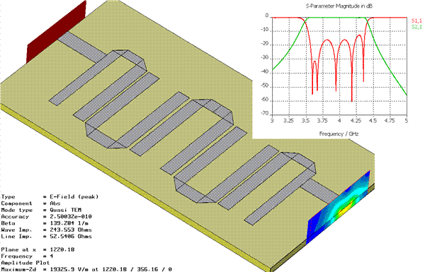
In the picture number 1 we can see a
hairpin filter. This filter is a structure that uses parallel-coupled lines. In addition, we can
observe the angled bends, this angles are common to stripline designs and represent represent a
compromise between a sharp right angle.
If we plot S-Parametres of this filter:
In the following picture we can find a
solution for delay signal problems. We enlarge a path to synchronize the signals
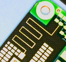
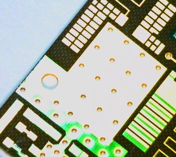
Via stitching is a technique used to tie
together larger copper areas on different layers, in effect creating a strong vertical connection
through the board structure, helping maintain a low impedance and short return loops.
In RF designs stitching is used in combination with guard rings to create a
via wall, helping create an electromagnetically 'quiet' PCB. Via stitching
can also be used to tie areas of copper that might otherwise be isolated
from their net, to that net. In the PCB I found a case of via stitching:
Mechanical holes are very important to fix the PCB to the mechanical structure:

I designed a Dimmer. These are devices used to lower the brightness of a light. By changing the voltage waveform applied to the lamp, it is possible to lower the intensity of the light output. Although variable-voltage devices are used for various purposes, the term dimmer is generally reserved for those intended to control light output from resistive incandescent, halogen, and (more recently) compact fluorescent lights (CFLs) and light-emitting diodes (LEDs). More specialized equipment is needed to dim fluorescent, mercury vapor, solid state and other arc lighting.
4.1.
Objectives
This project is the most important part in the course and I think it has teach me a lot.
I have learn about mechanical, electronic, system, sales and managment engineering.
I think the most relevant objectives are:
-to improve organization skills
-to manage multiple CAD software to make a product
-to improve skills to make decisions and optimize time and costs
-to approach us to the real industry world
-to increase knowledge about the electronic market
-to introduce us to the management of a project
4.2.
Flow work
This section show how the project has been developped during the time:
-October: requirements definition and pre-prototype designs.
-November: circuit and PCBv0 design, mechanical designs.
-December: mechanical redesign and PCB placement and routing.
-January: assembly and final product.
4.3.
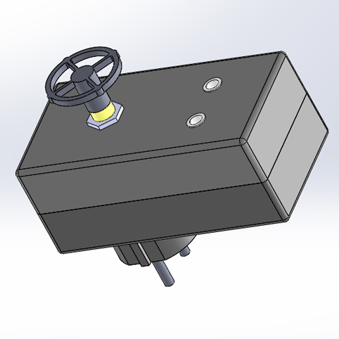
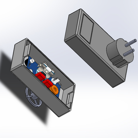
Mechanical design
Altium is a software which uses libraries to organize components and their properties and sources. When you do a project with this software you must create yourself the libraries to make your project portable. The following button allow you to download my libraries made for this project:
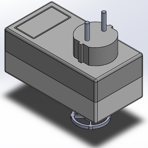
The followings images show
the final mechanical design:

4.4. Electronics design
Altium is a software which uses libraries to organize components and their properties and sources. When you do a project with this software you must create yourself the libraries to make your project portable. The following button allow you to download my libraries made for this project:
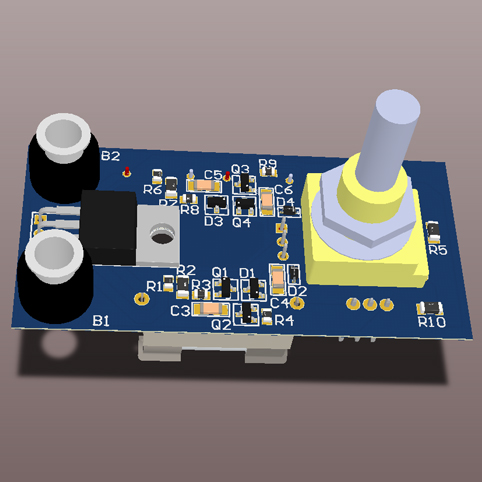
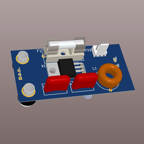
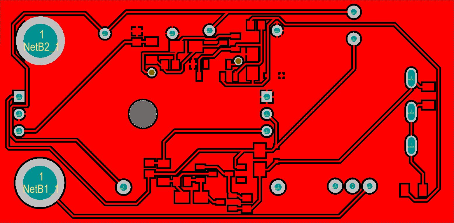
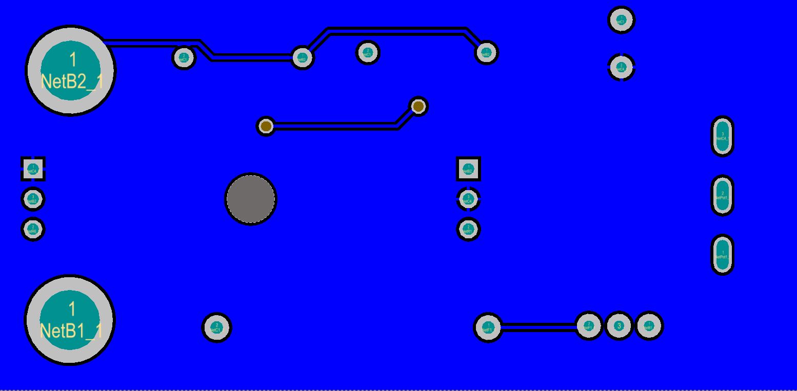
You can see the PCB in the
following images:
3D view:
Top layer:
Bottom layer:
4.4.1. Electronic simulation
Electronic simulation is
done to check if the design of the circuit works. In the following video you can see how if the potentiometer
is regulated the output signal changes her amplitude:
4.5. Libraries (Schematic + 3DComponents
+ Footprints)
The following buttom allow you to download the libreries used to make this product.
4.6. PCB Design
If you want to open this project in Altium you can download it with the buttom below:
4.7.
BOM
| Component | Quantity | Price per unit | Subtotal | Supplier |
|---|---|---|---|---|
| MMBT2907AT-7-F | 50 | 0,09 | 4,5 | RS |
| MMBT2222ALT1G | 2 | 0,1 | 0,2 | RS |
| 1N4148WS-V-GS08 | 2 | 0,053 | 0,106 | RS |
| Triac TS820-600T | 2 | 0,88 | 1,76 | RS |
| Diode Zener BZX84C15 | 2 | 0,14 | 0,28 | RS |
| Fuse | 10 | 0,741 | 7,41 | Sonytel |
| Potentiometer 220 k / 1 W | 1 | - | - | - |
| C1 100nF / 400V | 2 | - | - | - |
| C 1 uF / 25 V | 25 | 0,09 | 2,25 | RS |
| C 10 nF / 25 V | 25 | 0,558 | 13,95 | RS |
| R 10 k / 0.125 W (0805) | 4 | - | - | Laboratory |
| R 50 k / 0.25 W (1206) | 2 | - | - | Laboratory |
| R 20 k / 0.125 W (0805) | 2 | - | - | Laboratory |
| R 1 k / 0.25 W (1206) | 1 | - | - | Laboratory |
| R 360 K / 0.25 W (1206) | 1 | - | - | Laboratory |
| TOTAL | 30,456 |
4.8.
Providers
![]()
RS Components
es.rs-online.com
![]()
Molex
www.molex.com
Sonytel
Calle de Manuel de Falla, 3, 18005
Granada
4.9.
Conclusions
If you think you are going to finish this bachelor without to know how to implement your projects into a real concept. Do this course, you are going to learn professional softwares which are used all over world.
The teacher will give you the knowledge to design a complete product with a correct protocol to obtain a good final result.
4.1.
Description
It is a voluntary project. 8 team members built a musical instrument able to play
7 notes.
4.2.
Electronic design

The main component is a LM555 which is able to generate the frequency necessary
through the capacitors a resistors configuration chosen. In this case 493.88 Hz.
The signal form is:
