PRINTED CIRCUIT TECHNOLOGY
Rosa Mariana Martínez Mora
Rosa Martinez Mora

Degree in Telecommunications Technology Enginering of the University of Granada.
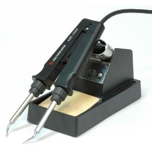
Techniques hot-air welding
The process of SMD desoldering and soldering is necessary to buy tools and specially designed instruments for this as calls thermal tweezers for work in SMD two ends that make soldering or desoldering work something simpler. Simply take SMD place the clamp element in the circuit and turn your heater with temperature control for precise and accurate work.
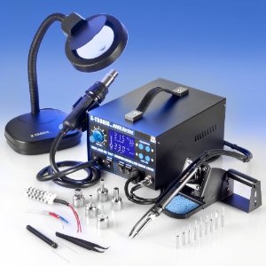
But the above is only for those who have two legs SMD. When you have to perform work on SMD and also with SMD connectors Soldering Station Hot Air is used to control temperature and air flow allowing work on these circuits to perform. That station for welding by hot air jet can be used to extract and mount many types of components as well as for drying, plastic welding, preheated among many other applications that make the welding station an inseparable tool of modern workshop electronics.
Welding Techniques / desoldering made
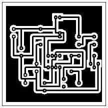
Recognize elements on a PCB
Proyect: VÚMETRO
Objective of the project
In this proyect is to develop a vumetro. This instrument is an indicator device in audio equipment to display the signal level units of volume, it is sometimes also called volume indicator.
It will be composed of several LEDs that will turn on or turn off due to the received speech. It will use a microphone and the integrated LM3916 with 9V. First, I will do the pcb using the Altium software due to this is an important software to buildt the PCB. Then, I will use other program- Solid Works- and this is important to do the mechanical design to the box.
Phases of the design process followed
Once the project is chosen to perform, the next step is to perform the electrical circuit.
If you have already done enough testing and to have chosen the parameters of resistors and capacitors correct, the project gets into a speaker.
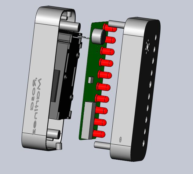
After this design, I must think about the box that envelop our PCB.
I do a rectangular design according to the possition of the LEDs and then, I put the PCB in the box to check that the dimensions are good.
Finally I buy the materials and I will do the actual manufacturing.
A graffic with the phases performed is the design phases are
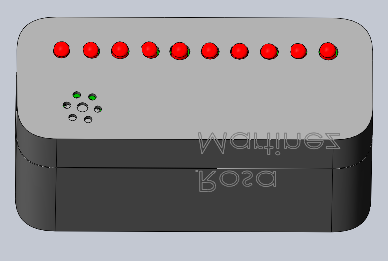
Mechanical Design
At first, I did not know how we would be the size of the PCB so it was a simple box with Solid Works software that I was chaged the parts.
The box has dimensions of 90x37mm and it es formed by a bottom with 5,6 mm height and its cover by a top with 3,68 mm height.
The edges of the box are made with a conical curve of radius 10mm. It contains various structures for the subjection of the box.
This structures are: Several tubes of differents sizes that serve as subjection to the plate.
Also, several holes were designed in a row at the top of the box so that it could be the lighthing of de LEDs.
To be heard appropiately speaker sound , I will be held at the top a small hole with the form according.
Also, I will use several tubes that will serve for the top and bottom remoin embedded. The stack is placed 1mm below to the PCB.
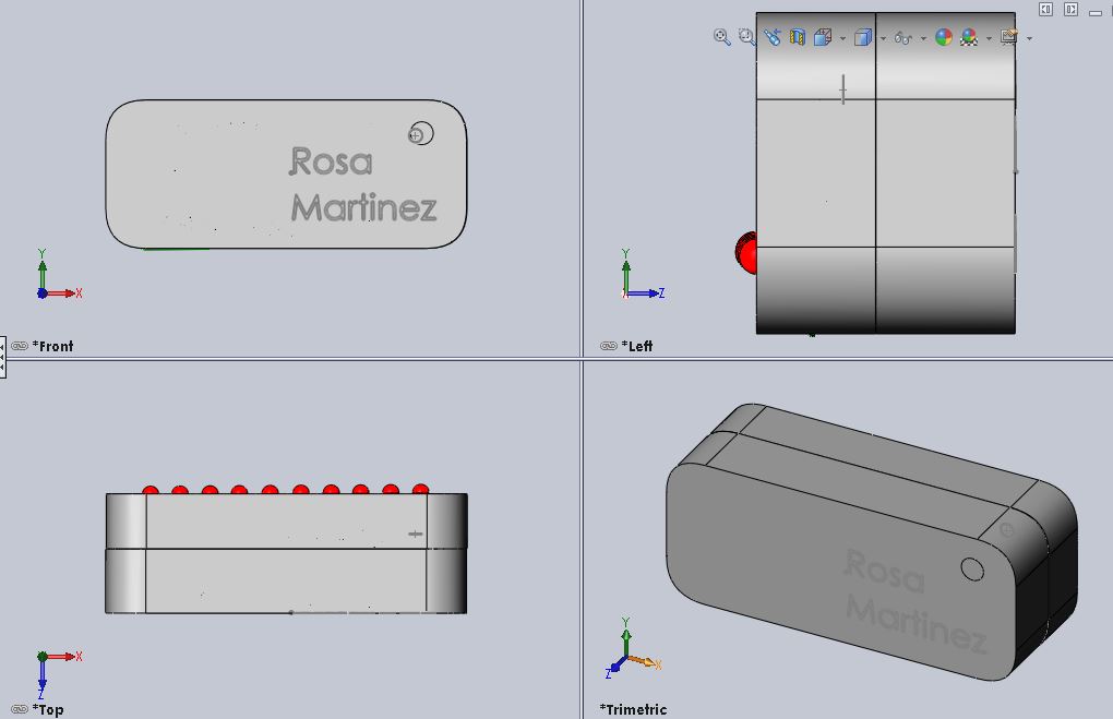
The dimensions of the design are
If you want to see a video of the proyect+pcb you have here this link
If you want to see the center of mass, you can check the following link
Electronic design
For our electronic design I will use the Altium software, which also allows us to perform simulations and it is a very powerful tool that also we use to create the PCB
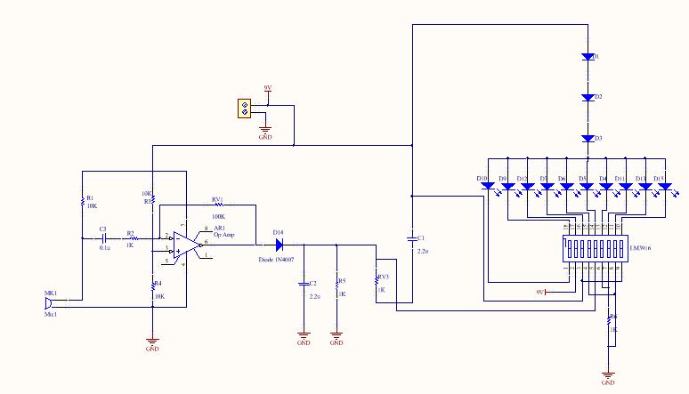
The VU meter circuit simulations is as follows:
The circuit consists in an integrated receiving an audio signal via a microphone. With such a signal output are switched which are connected LEDs, so depending on the sound level will be switched more or fewer pins.
An amplifier will be included after the microphone. An envelope detector is placed. The capacitor stores charge when the input signal increases and slowly discharge through the resistor when it decreases. The diode ensures that no currents is flowings in the opposite direction to the input circuit. With this, an AC audio signal is converted into a DC signal pulses.
Due to the three diodes in series ensures, there is enough voltage drop to drive the LEDs and resistors avoid putting.
Once the idea was conceived and running our circuit, we should know what components would be in our project. To do this, we look datasheets of diferents products to find items that we seem corrects.
The datasheep of differents components are the next:
Also I have donde a simulation with Proteus software and this is the result
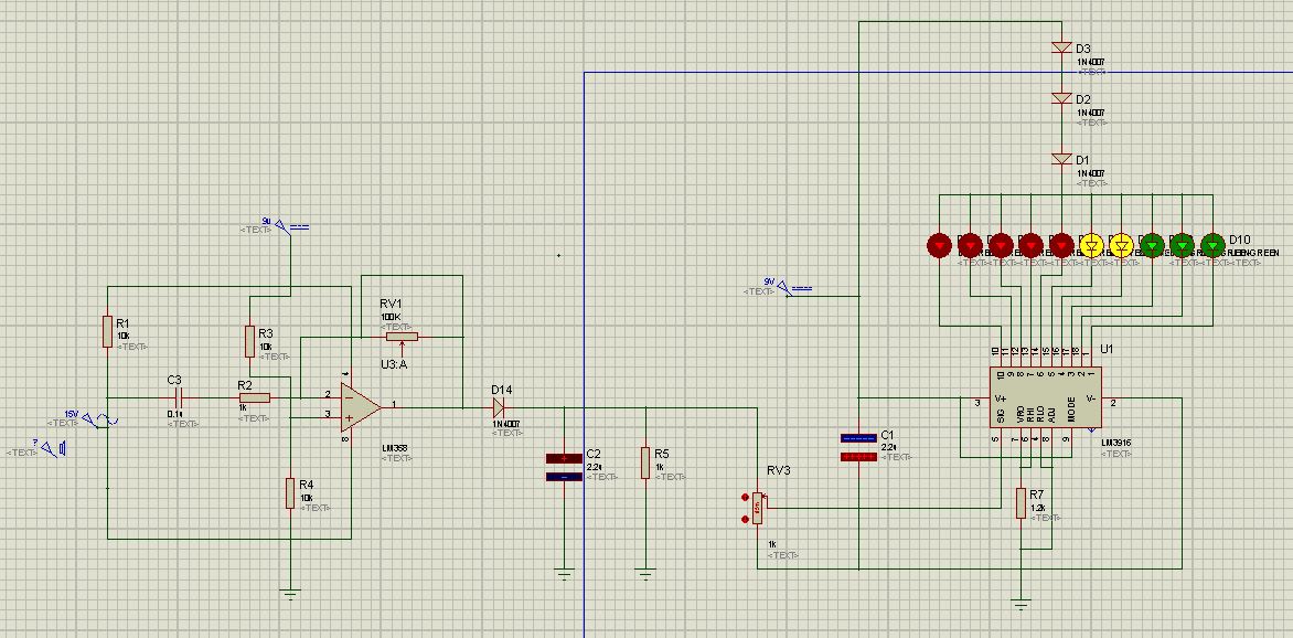
Circuit elements (SCH + PCB + 3D) project
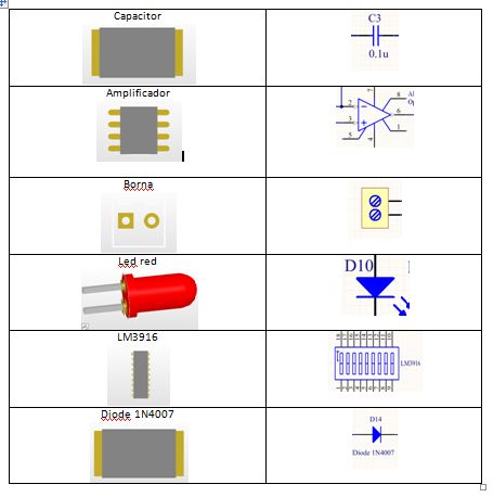
After choosing the components, we should get to have all our items in libraries Altium. By searching through the forums of the program and how to create the footprints measuring the pinout and size of our components we create the footprints. We did the schematic of our approach indicating the different parts of our operation and information to complete the templates.The libraries used for our design are:
"Below a link to the project in altium (schematic and pcb) is shown" schematic
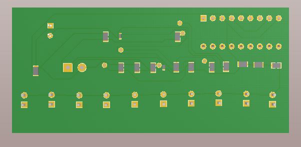
Also we can see the differents footprints to the many components in this image:
You can pick in this link
PCB design
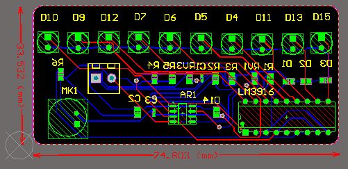
Already with our components, we turn to design the PCB.
We will consider using our knowledge of PCB layoutof tracks such as land trying to go around the outside of the circuit, do not make right angles to the tracks, no SMD components are on the TOP, our screen printing is the correct and that do not cross the tracks.
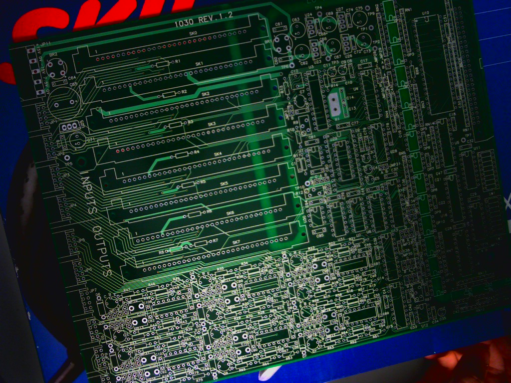
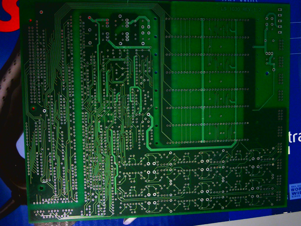
First, elements are positioned. Once placed and routed our components, we have the following PCB.
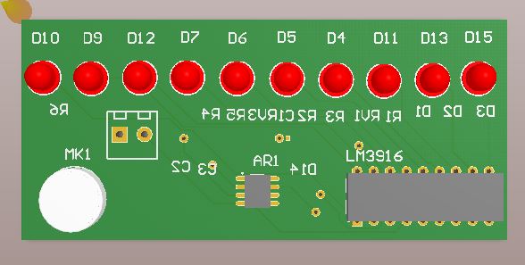
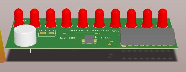
3D Design
Here you can see how it looks 3D PCB design in Altium program.
You can see a video with the pcb:
BOM
Below is a table with the prices of purchased materials and the total cost is presented
| Quantity | Product | Price(Euros) | Total(Euros) |
| 3 | Resistors10k | 0,2 | 0,6 |
| 4 | Resistors1k | 0,15 | 0,6 |
| 1 | Resistors100k | 0,2 | 0,2 |
| 1 | Mik | 2,42 | 2,42 |
| 1 | Condensador 0,1u | 0,012 | 0,012 |
| 1 | Condensador 2,2u | 0,012 | 0,024 |
| 1 | Diode 1N4007 | 0,11 | 0,11 |
| 3 | Diodes | 0,1 | 0,3 |
| 10 | LEDs red | 0,2 | 2 |
| 1 | LM3916 | 2,05 | 2,05 |
| 1 | Battery 9V | 2,55 | 2,55 |
| 1 | Battery Holder | 2,88 | 2,88 |
| TOTAL | 13,74 |
A BOM with the approximate cost for a product is the following:
| Phase | Hours | Price per Hour (Euro) | Price Phase (Euros) |
| Design Requirements | 15 | 15 | 225 |
| Design Model | 5 | 15 | 75 |
| Simulate Model | 4 | 15 | 60 |
| Preliminary Design Model | 15 | 15 | 225 |
| Define Requirements | 8 | 15 | 120 |
| Design Prototype | 20 | 15 | 300 |
| TOTAL | 1005 |
Service provider of different material acquired
The components can be purchased at any shop. Those who do not succeed are searchable online. In my case I will use SONYTEL GRANADA but you can also find components eBay.
The manufacture of the plate would be done with the material and instrumental University. Likewise, for the box and lid, the 3D printer University would be used.
Pictures of the actual project
In the following pictures you can see our actual cash. To do this we had to spend our design soli-work to Cura software. Thus, by a 3D printer we have obtained the following result
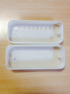
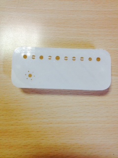
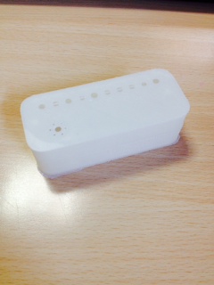
You can see how the design is correct. But you can also see some imperfections. These may be due to the 3D machine itself or it can be due to any errors in the design of the piece in solid works.
The holes in the top fit well and are all correct. But you can from inside the box have appeared a number of 'threads' in which there are to do well the inner tubes which united the piece.
Therefore, for the union of the piece is correct I will use Silicone.
Visit
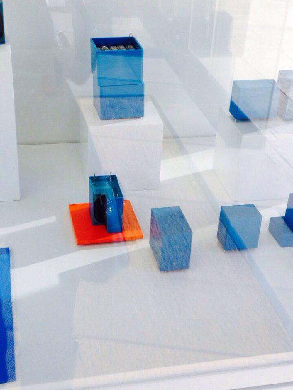
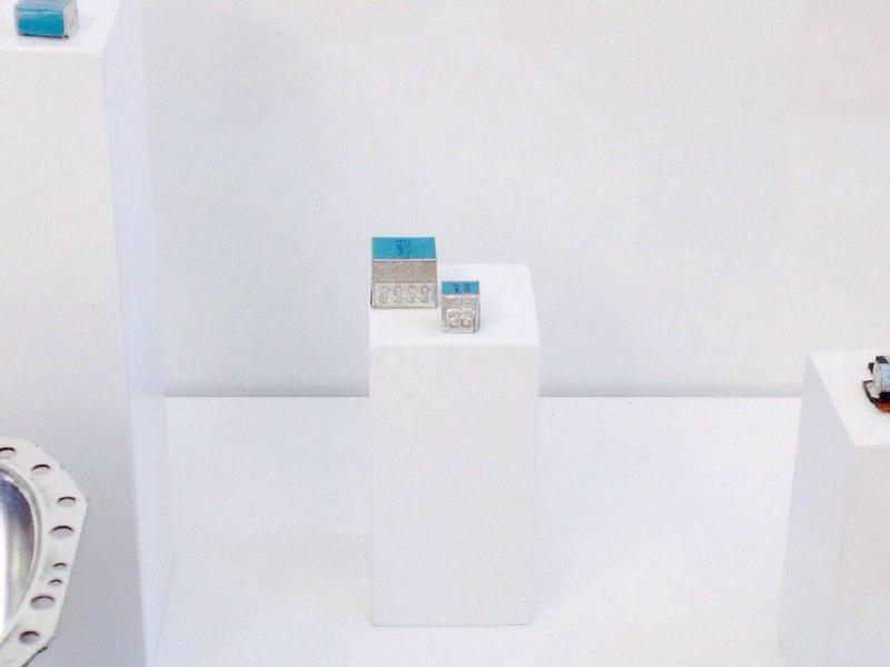
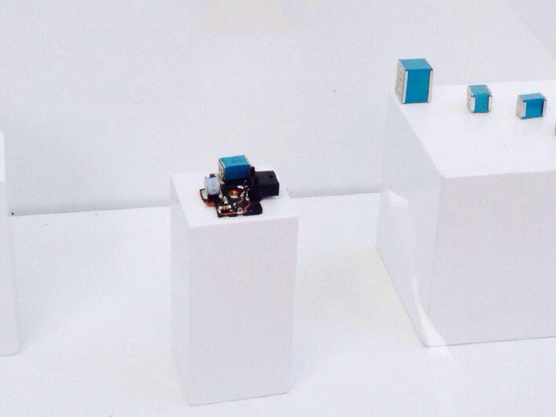
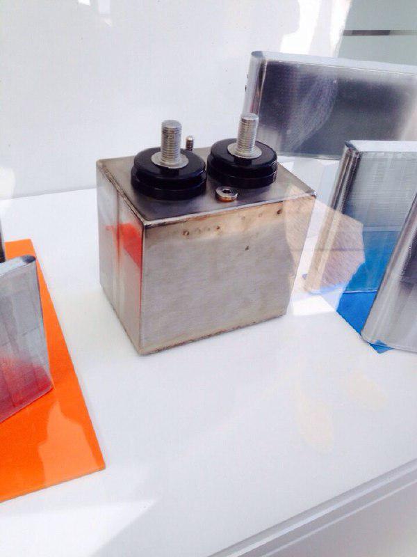
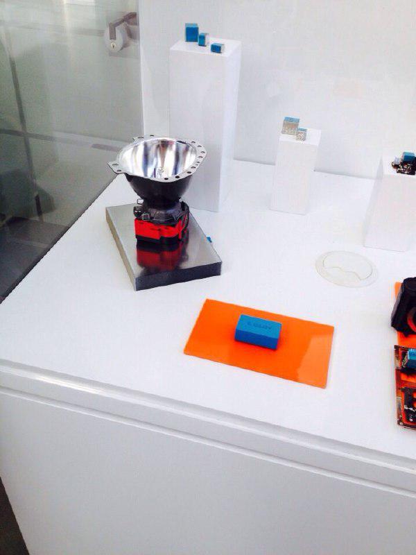
We had a visit to Malaga to visit some bussines: Aucore, Anova and TDK. We can see some images from this visit:
Conclusions.
In this project I have invested much time, since before the subject of Printed Circuit Technology had a complete lack of technology circuit manufacturing, also my problem was that I am not the speciality of Electronic joined so I didn't know things related more specifically to the electronics itself issues.
I've known Tell the pcb but also we have tried to bring the reality of all this, which is the process of manufacture
It was very important to think about the set design pcb + box since these concepts were practically united. Has been complicated and laborious learn various new software that I could use in other subjects. Although it is really gratifying to see that with effort and a little ingenuity, we can design a product in the beginning.
Future improvements
One possible improvement project would put different colors LED diodes in parallel so that also may be a more interesting and novel apparatus for the users.
Assessment work done.
In this work we have implemented many of the concepts learned in this and other subjects, from something as basic as solving an electrical circuit simulations of circuit behavior to something more complex as making a PCB by applying the concepts learned in the subject and also implementing knowledge of graphic design when making the case that this in other subjects of the race come to teach not making it impossible to work with them throughout the race.
From my perspective I learned a lot about electronics in general and I had a complete lack of more complex things electronic. You can also see how something that at first seems simple can be very complicated, so we see problems that happen in real life, albeit on a small scale, so they can develop skills to overcome these problems.
The work brings us to something more practical and that we can find to finish the race and learn that all is not studying, but apply different skills learned during our stage students.