
Printed Circuit Technology - Course Report

Víctor Burgos González
Contents
1. Introduction to PCT
2. Practical works - Laboratory
3. Copper-clad project
4. Integrated project
5. Soldering Instructor
6. Final conclusion
Printed Circuit Techology is an optional subject that can be studied in the last year of the Bachelor's Degree in Telecommunications Technology
Engineering (Electronics Systems's Specialization) of the University of Granada. Here ,
you can see the contents of the course, and the main web of this subject here where you can found the information and download the most important content of this subject.
The objective of this subject is to teach the main tools and the know-how of a electronic device, from the begining (idea) to the final step(retirement.
In this report I want to show what I could make and learnt in the course of this subject
teached by Andrés Roldán Aranda.
2. Practical works - Laboratory
In
this chapter I will share the work developed in the laboraroty of this subject. We use diferent solder stations to solder and disolder components, depends on the type of soldering (SMD, Trough-hole, BGA).
2.1. SMD
SMT (Surface-mount technology)Surface-mount technology (SMT) is a method for
producing electronic circuits in which the components are mounted or placed directly onto the surface of printed circuit boards (PCBs).
An electronic device so made is called a surface-mount device (SMD).
2.1.1. SMD soldering
In
the following video you can see the process which I soldered a SMD device in the laboratory of this subject. To solder this component, I used the AOYUE Int 2703A+
2.2. Through-hole
Through-hole technology , also spelled "thru-hole", refers to the mounting
scheme used for electronic components that involves the use of leads on the
components that are inserted into holes drilled in printed circuit boards (PCB)
and soldered to pads on the opposite side either by manual assembly (hand
placement) or by the use of automated insertion mount machines. (Extracted from Wikipedia)
2.3. Desoldering in the laboratory
The following photos show some of the devices that I have desoldered in the laboratory. I have chosen the most different packages in order to practice with the more of the desoldering technologies:
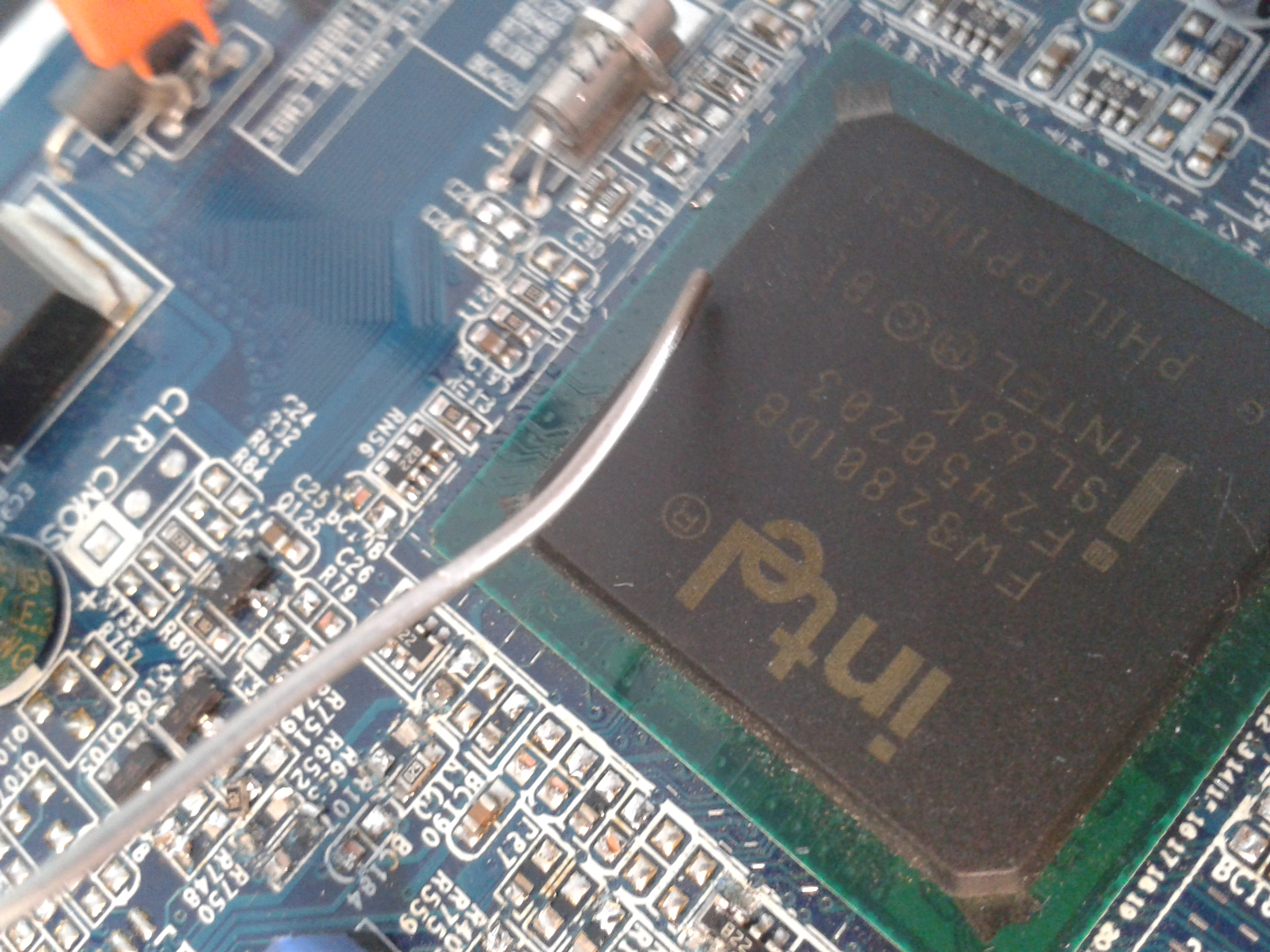
2.4. Infrarred desoldering
Using a the desolder rework machine (infrarred technology)ERSA IR 500 A
I desoldered a Microchip of Intel which has a melting point of:
Lead solder balls' melting point: 180 degree (advise: 210~215)
Lead free solder balls' melting point: 217 degree (advise: 235~245)
The following videos show the process, first desoldering and later cleaning the BGA after desoldering process, in order to reuse it: (Sorry for the bad quality of the videos)
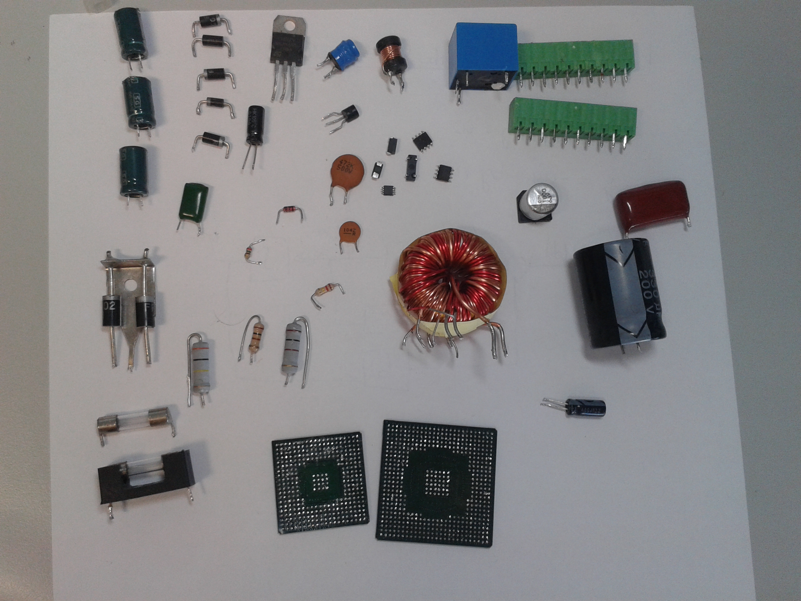
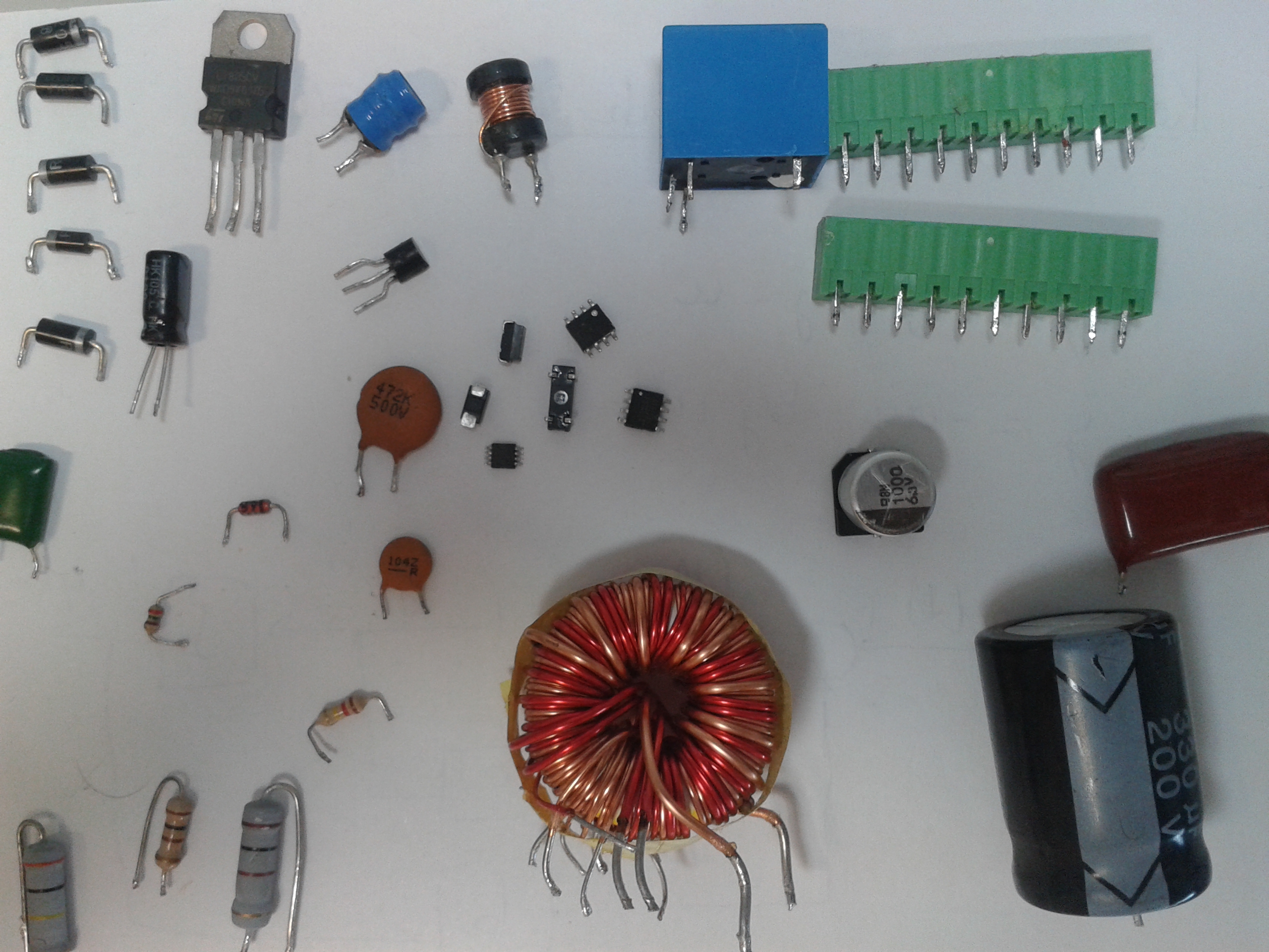
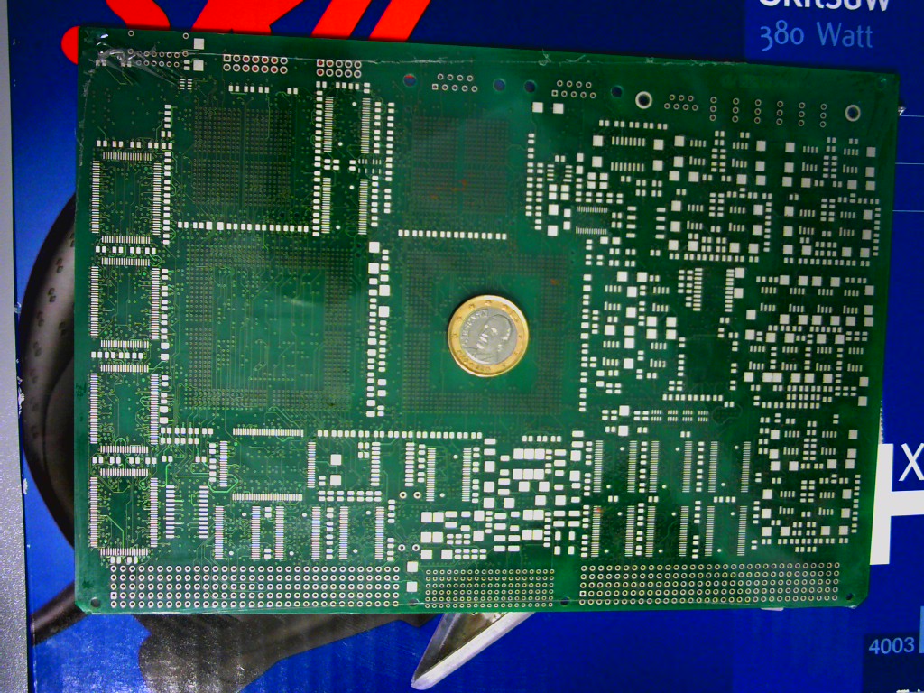
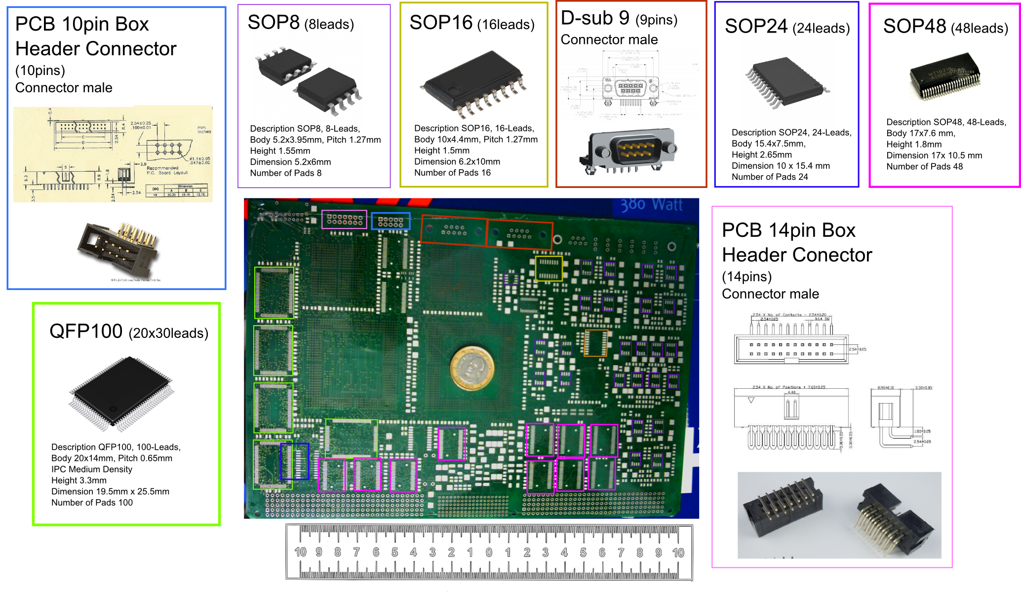
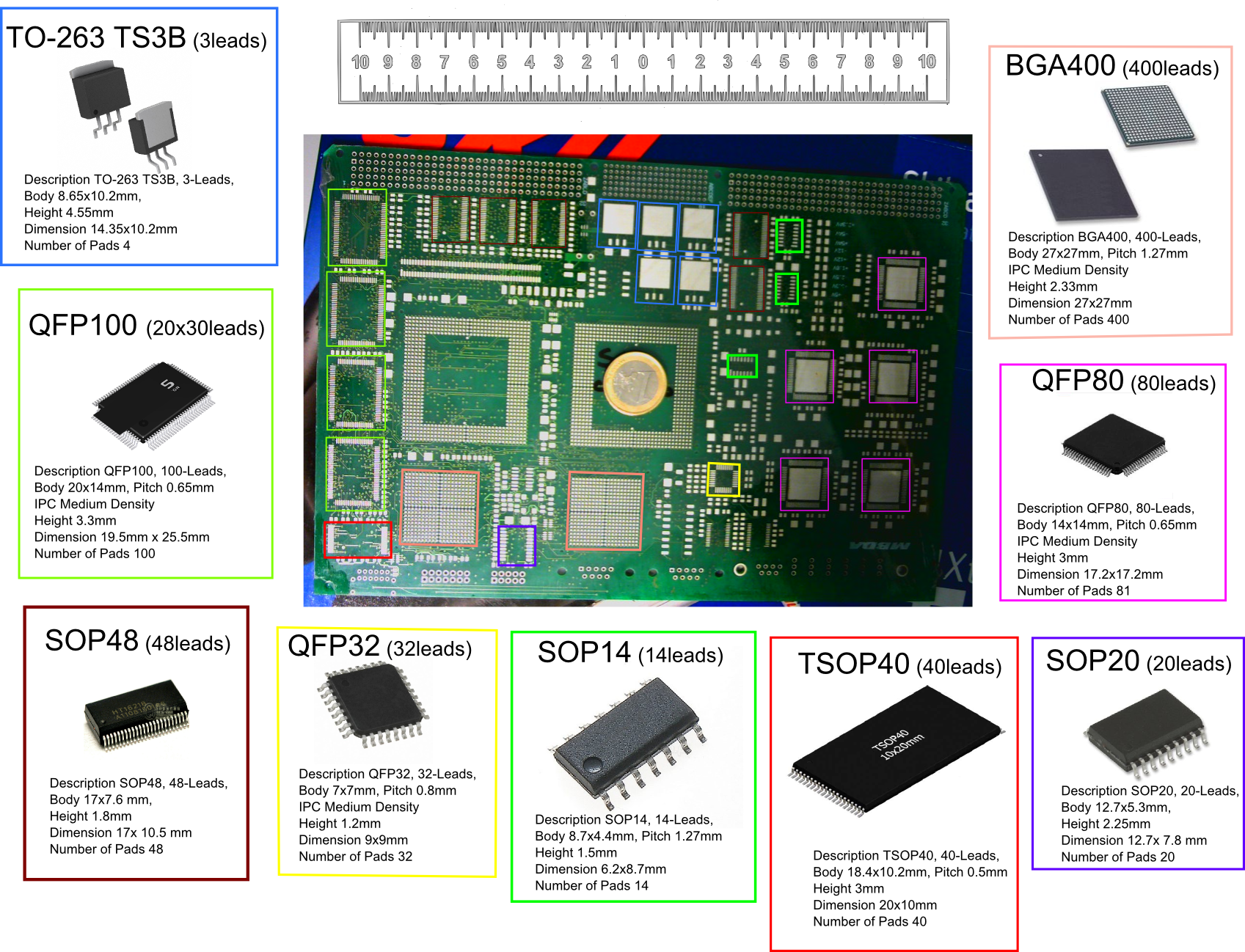
2.5. Examination and recognition of the elements of a PCB
In order to improve the knowledgement about the devices
,their packages and footprints, we have to do a recognition of the footprints of a PCB.In following days I will do this homework and share with you my knowhow about this components.
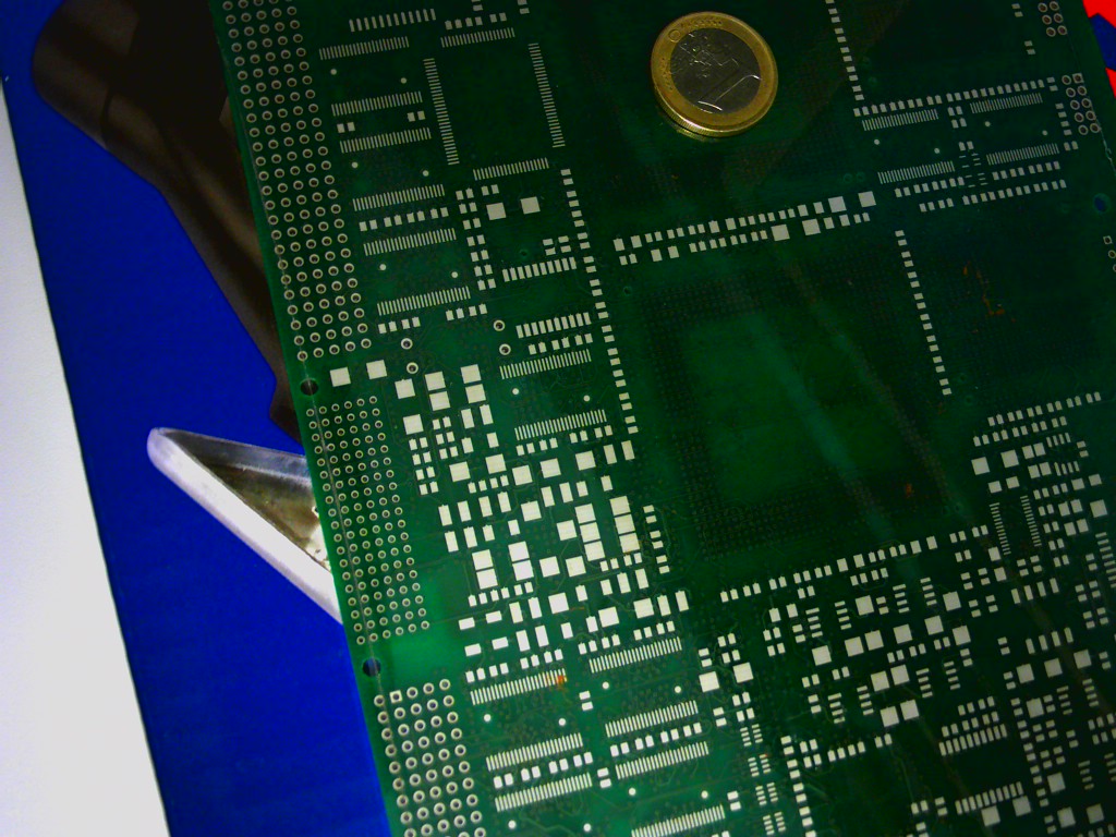
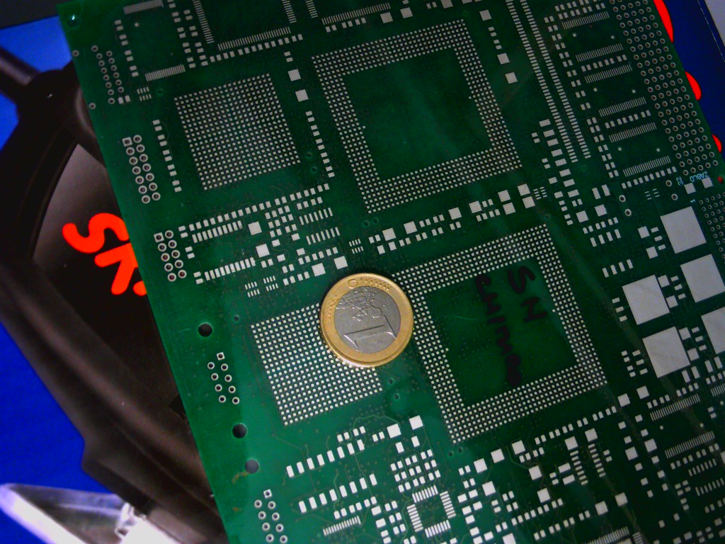
The
following images show the PCB:
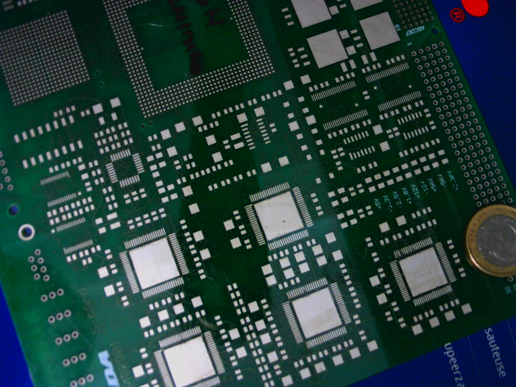
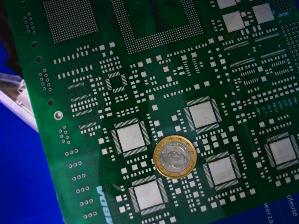
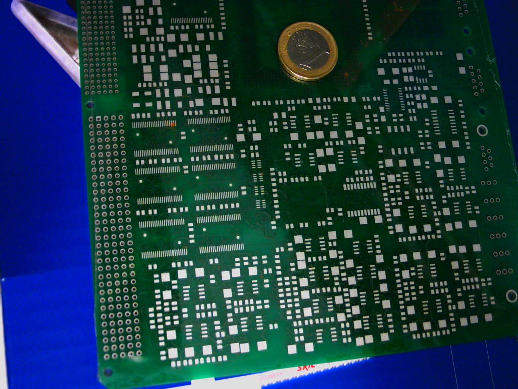
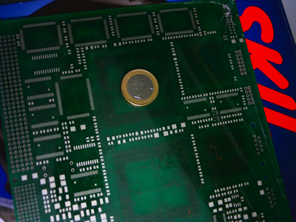
Some of the packages recognaised are:
The copper clad project has the origyn in a practical lesson about the copper clad soldering. A type of solder which you adquire some knowledgements about mechanical, electronics, 3D design, PCB, etc. Some of the students of this course decided to do this project (voluntarily) and we formed a great team. The project is based on the video of this website,so we decided to do a "piano" which was played it with the shadow of our hands.
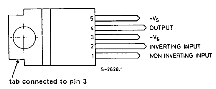
Every student had a part (musical note) of this project, but mine was the amplifier and volume control of this instrument. The following image shows the circuit of my copper clad design:
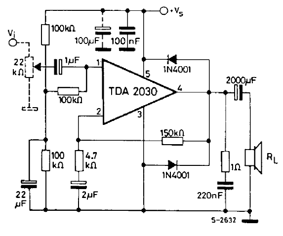
Device used as
aamplifier was the TDA2030 with the following connection diagram:
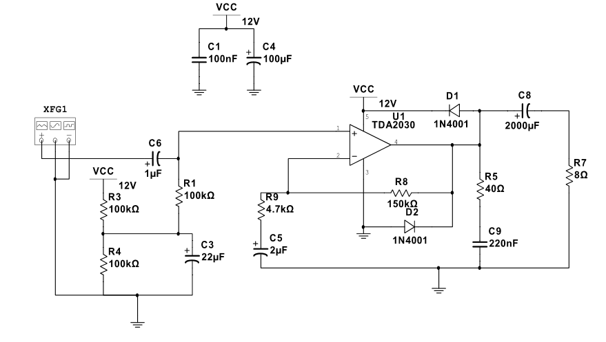
And I had to simulate in Multisim (in order to prove the correct functionanbility of the system) with this circuit:
Finnally, some videos of the test and the final functionality with the circuit of a classmate:
4.1.
Introduction
This project let us to know how is the real life of a product, from the beginning to the end. We have to define the requirements,
design the model, build it and test it. We have to make a merkating work too, in order to know the situation of a
engineer in the world of the technology.
My project is MOL (Music Organ Led) based on this project from Instructables. I contacted with the autor to ask for some information and
he sahre with me some of his knowledgement. Is a device which turns on some led following the frequency of the music.
The main objectives of this project for me are:
-to improve my organization skills
-to manage CAD software (Altium and SolidWorks)
-to give us the know-how of the management of a project and industrial world
-optimize my time and costs of the products (electronic market)
The flow that I have follow in this project is:
-October 2014:
-requirements definition.
-pre-prototype designs.
-November 2014:
-circuit and PCB v0 and v1 design.
-mechanical design v0 and v1.
-December 2014:
-mechanical redesing until v5.
-PCB placement and routing until v6.
-January 2015:
-final design.
-assembly.
-final product.
4.2.
Mechanical design
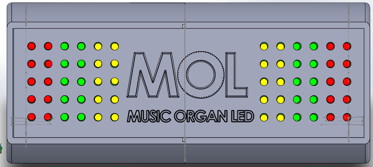
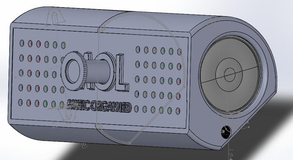
This mechanical design is composed of three parts forming an assembly:
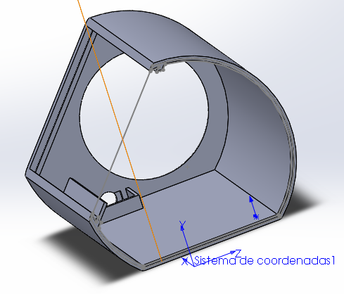
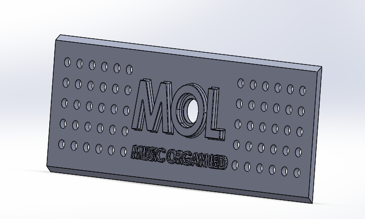
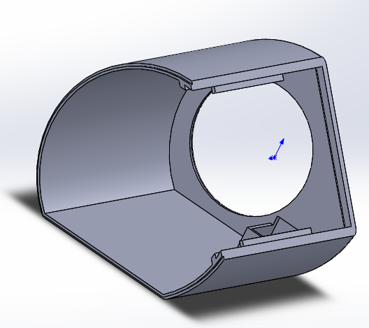
Some images of the design of the assembly in SolidWorks:
Video of 3D model:
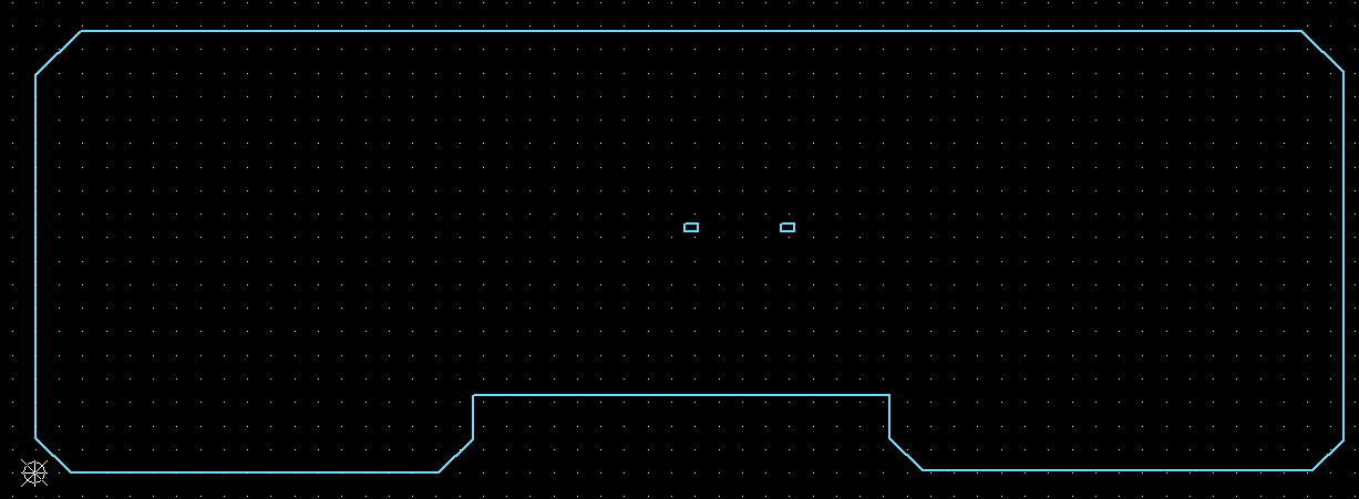
Now, the documents which show the mechanical design and it dimension:
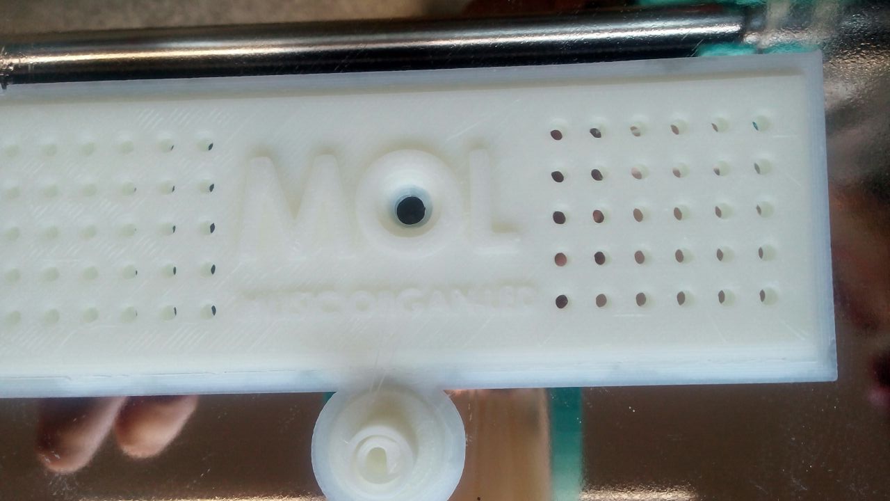
The first 3D printed part of this design:
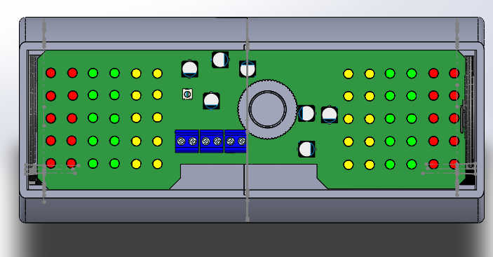
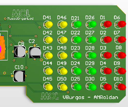
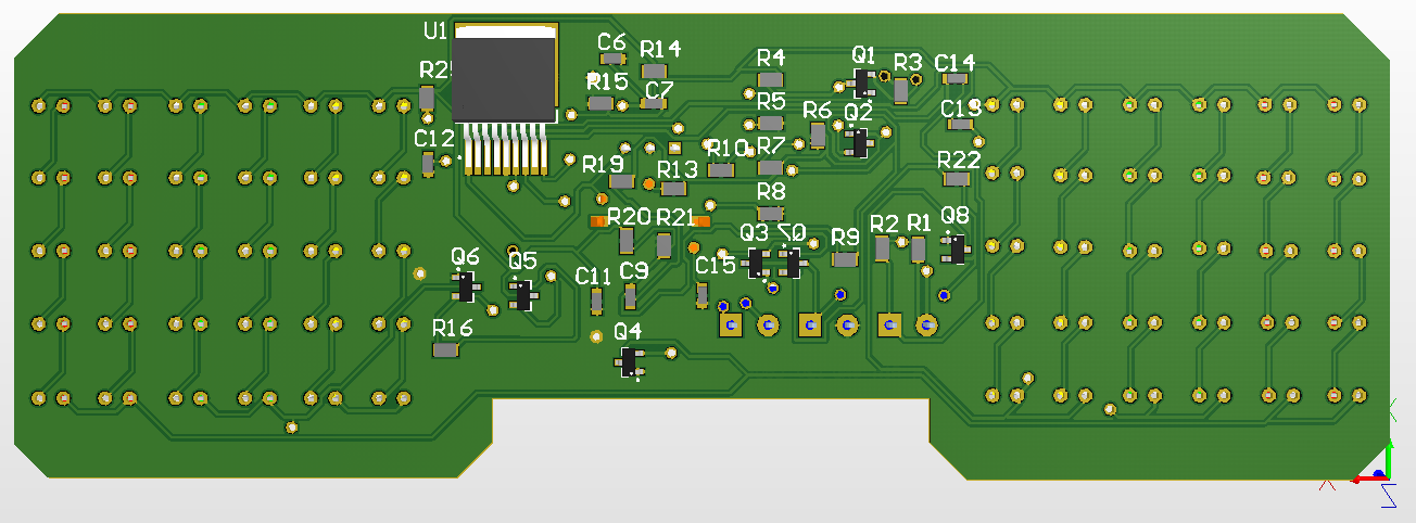
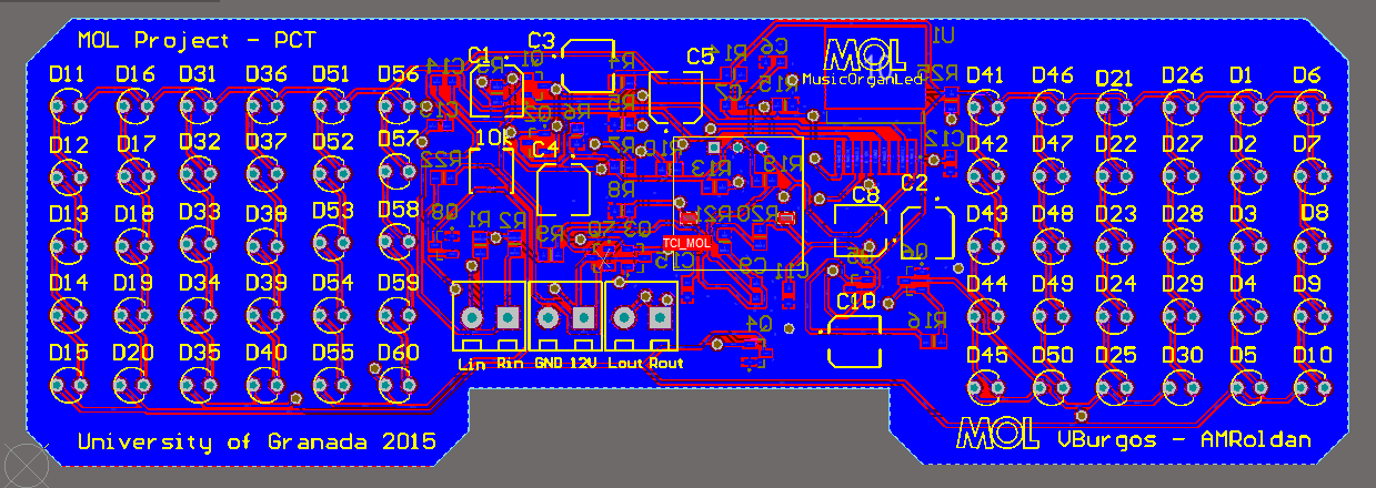
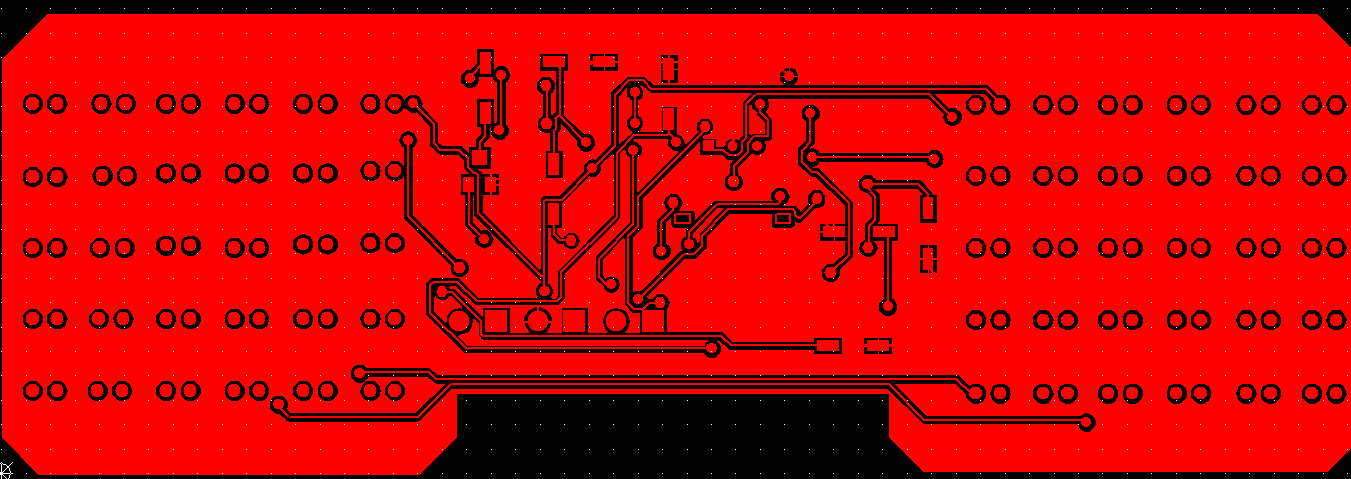
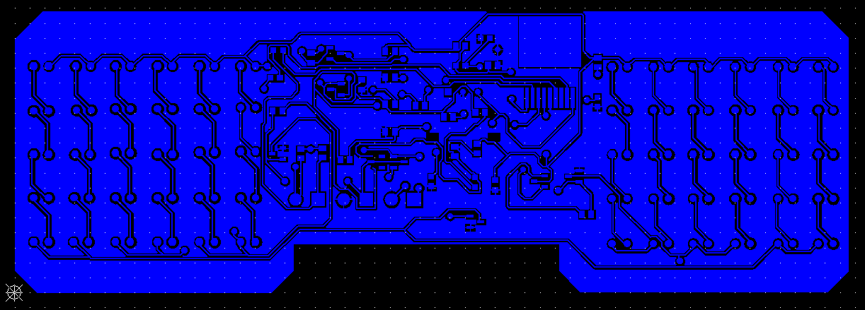
4.4. Electronics design
Some images of the design in Altium Designer (2D and 3D view):
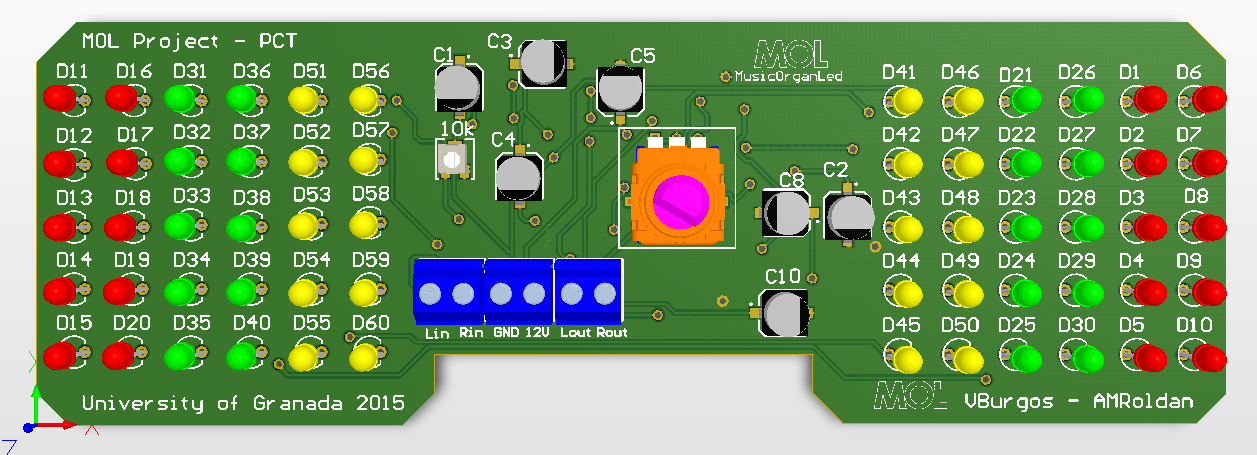
Logo incrusted in PCB following the manual given by the professor:

Video of 3D model in Altium Designer:
Now, the gerbers generated in order to build the PCB:
4.5. Libraries (Schematic + 3DComponents
+ Footprints)
[This part will be filled in the next version]
4.6.
BOM
4.7.
Providers
![]()
RS Components
es.rs-online.com
Sonytel
Calle de Manuel de Falla, 3, 18005
Granada
4.8.
Real images result
Here you can see
some photograps of the project:


The following
video show how the product works:
4.11.
Improvements
-Redesign the filters in order to make it functional with 9V supply (batteries->portable)
-More filters in order to have a more beautiful result. (more filters, more colors)
-When you make a project like this and you need to buy the devices, if you buy more electronic components, it will be cheaper.
So, it may be cheaper buying more quantity of components.
The instructor homework has the objective of help to the classmates in some skills, for example, in my case was the soldering tools.
One of my first jobs was the introduction of the soldering station which we have in the laboratory. This machine has three technologies of soldeing/Desoldering devices
Hot Air Gun
Hot Air Gun
Hot Air Gun
Later, I had to prepare a manual presentation with the main steps and parts of the rework BGA machine IR500A. In the next PDF viwer you can see it. In the manual you will se some photos of the machine. I hope you enjoy it.
Now, I have finished this course and I can say that I have learnt a lot of new things. Since three months, I couldn't have said that I will be able to do something like my integrated project. A project where I have used new tools which help me in my future, for example, Altium Deigner or SOlidWorks. In my opinion, this subject is one of the most similar with our future job, because we have a project and we need to know how to make it real. Moreover, this subject should be annual, because there are a lot of contents to understand correctly inn only 3-4months. To finalize, I have to say that I'm really proud of my job, and I hope someday I will be able to build it.