|
A number of people have asked the question recently, Why
do we see changing volumes in our lead-free solder joints?
Although lead-free materials do have a different density they
are actually talking about the loss of solder to the component
terminations during reflow. During lead-free introductions it
is common, but not ideal, to use tin-lead coated component
termination either because nothing else is available or they
have been supplied without warning. Using tin/lead
terminations with a lead-free paste has been shown, in some
studies, to have an impact on joint reliability and also cause
secondary reflow on wave soldering resulting in lifted leads.
With a lead-free process solder paste is printed on to the
surface of the pads, most commonly 0.006 of paste is used.
Ideally one of the alternative lead-free printed board
finishes like gold, tin, silver or copper OSP is specified.
Lead-free solder levelled alternative like tin/copper/nickel
may also be considered to replace tin/lead and is by far the
most solderable coating depending of course on thickness.
Component terminations are then automatically placed into the
surface of the paste; the board then passes for reflow in the
normal way. During reflow the board passes through convection
or vapour phase soldering (VPS) process reaching and exceeding
a normal reflow temperature of 210-220°C used for tin/lead
assembly. In this situation if the component terminations are
tin/lead plated or dipped they will move into a liquid state
and are very wettable, probably more so than most alternative
PCB finishes and the alternative component termination plating
like tin and palladium.
 |
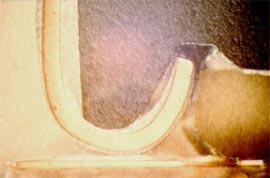
Example of tin/lead Wicking in VPS originally
featured in the Texas Instruments Surface Mount Hands-On
Workshop run by the author in Bedford during 1980s. This
resulted in an open intermittent joint.
When the lead-free solder paste reaches reflow temperature
at 217-220°C the solder is far more likely to wet to the
component termination particularly on leaded parts like SOIC,
QFP or PLCC. The board assembly will continue to rise to
235-245°C and hold until all the terminations are above reflow
for a minimum of 30 seconds. In the case of parts with leads
there is a large surface area to wet. The result is
Wicking a process defect that can occur
during normal tin/lead processes when the solderability of the
PCB is poor and the component very solderable. In the past it
was very likely to occur with convection and IR ovens with
mainly top heating and limited bottom heating. It could also
occur with mesh belt systems as the belt could hold the board
temperature down allowing the component termination
temperature to rise much faster. VPS originally exhibited this
type of defect more commonly on batch vapour phase systems
with no or poor preheat. In this case the lead terminations
would reach soldering temperature much more quickly than the
printed board.
 |
Example of tin/lead paste Wicking on copper OSP
board finish after reflow. This was due to incorrect PCB
cleaning which stripped the OSP surface protecting from the
pads.
Examples of Wicking on gold pads on a pocket
pager application with tin/lead paste when the solderability
of the pads was poor.
Example of a satisfactory lead-free joint but the
increased volume of solder can be seen on the surface of the
tin/lead pin away from the joint area.
In the case of lead-free reflow with tin/lead component
terminations the wicking process is practically the same.
However, it can result in the reported disappearing solder
contributing to the component coating and not joint formation.
Although many people will not have seen this type of defect
before it has been encountered and fairly well understood.
Its the lead-free aspect that may catch people out during
manufacture and final inspection.
Three images showing tin/silver/copper paste reflowing with
tin/lead component terminations exhibiting the wicking
effect.
|