MARIO LIZANA CALVO
 |
CONTACT:[1] marvic93@correo.ugr.es[2] mariolizanac@gmail.com |
ClapClapLamp project
DESCRIPTION
ClapClapLamp is a very useful product that can temporarily turn on and off a light in cabinets or lockers without touching to the main switch of the room. You only have to clap twice, ClapClapLamp will do the rest for you!
ClapClapLamp is designed to save time and electricity, it can run for several months and the batteries can be changed very easily.
MECHANICAL DESIGN
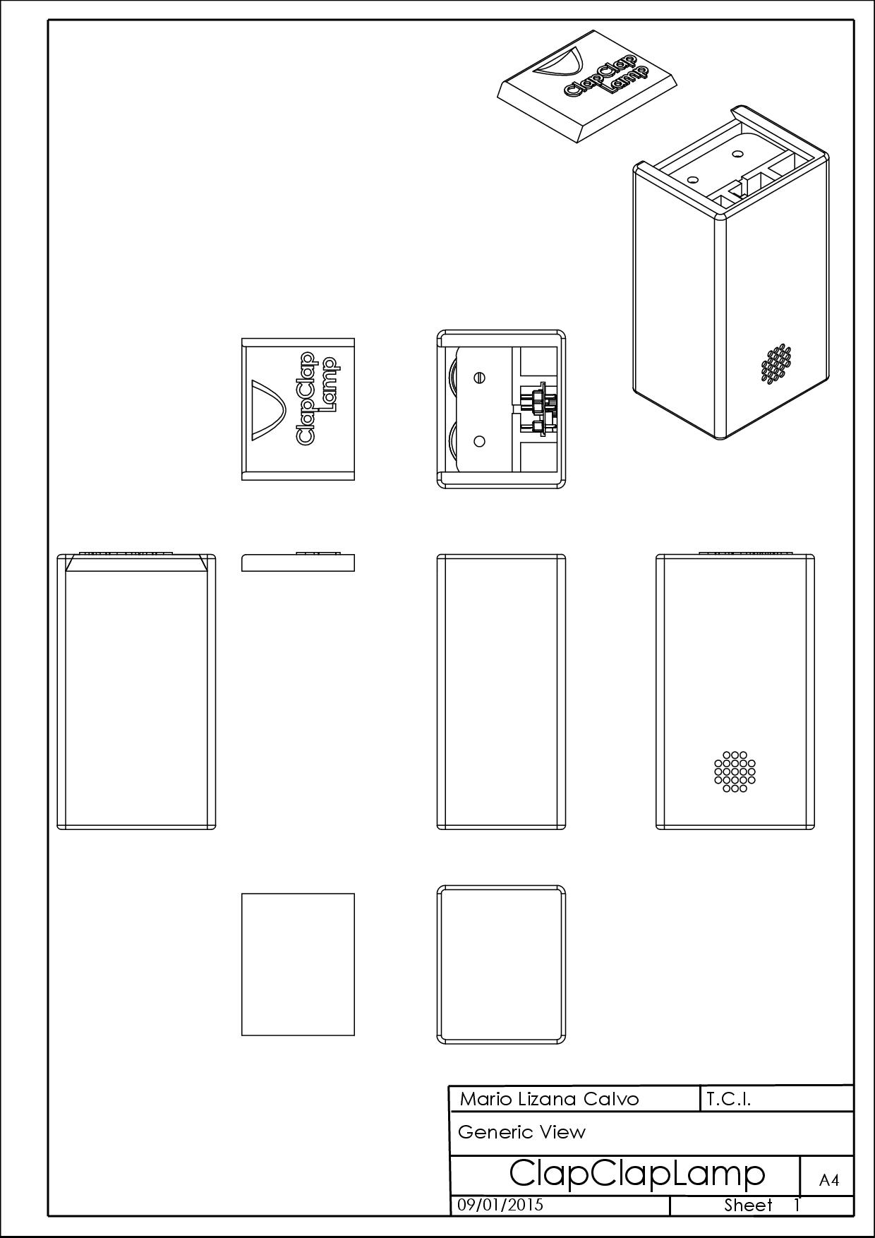
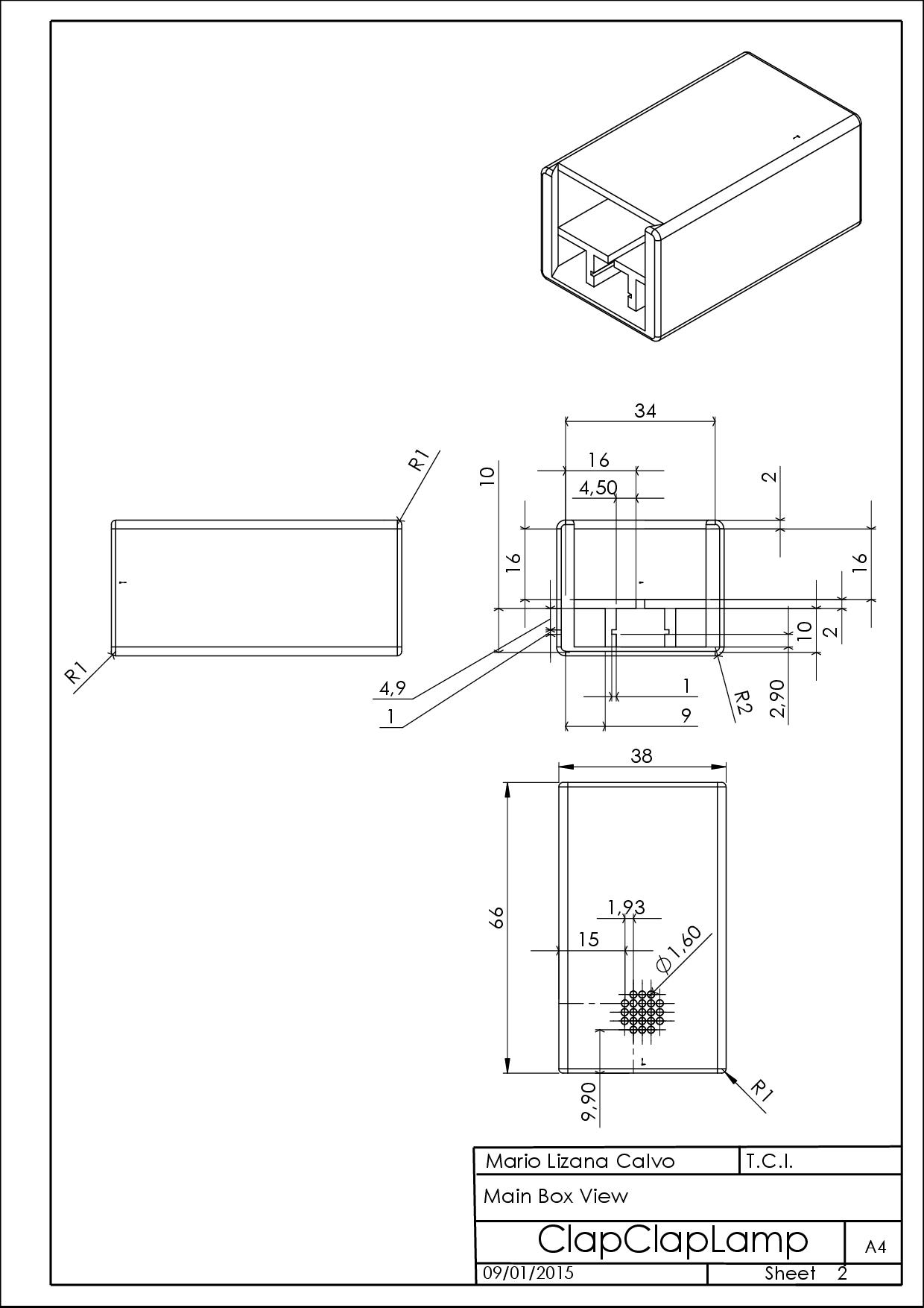
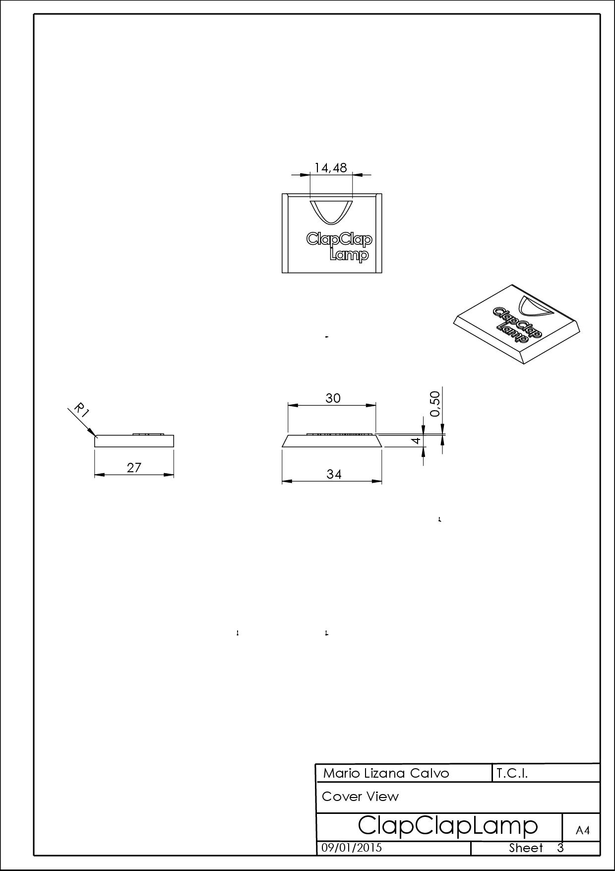
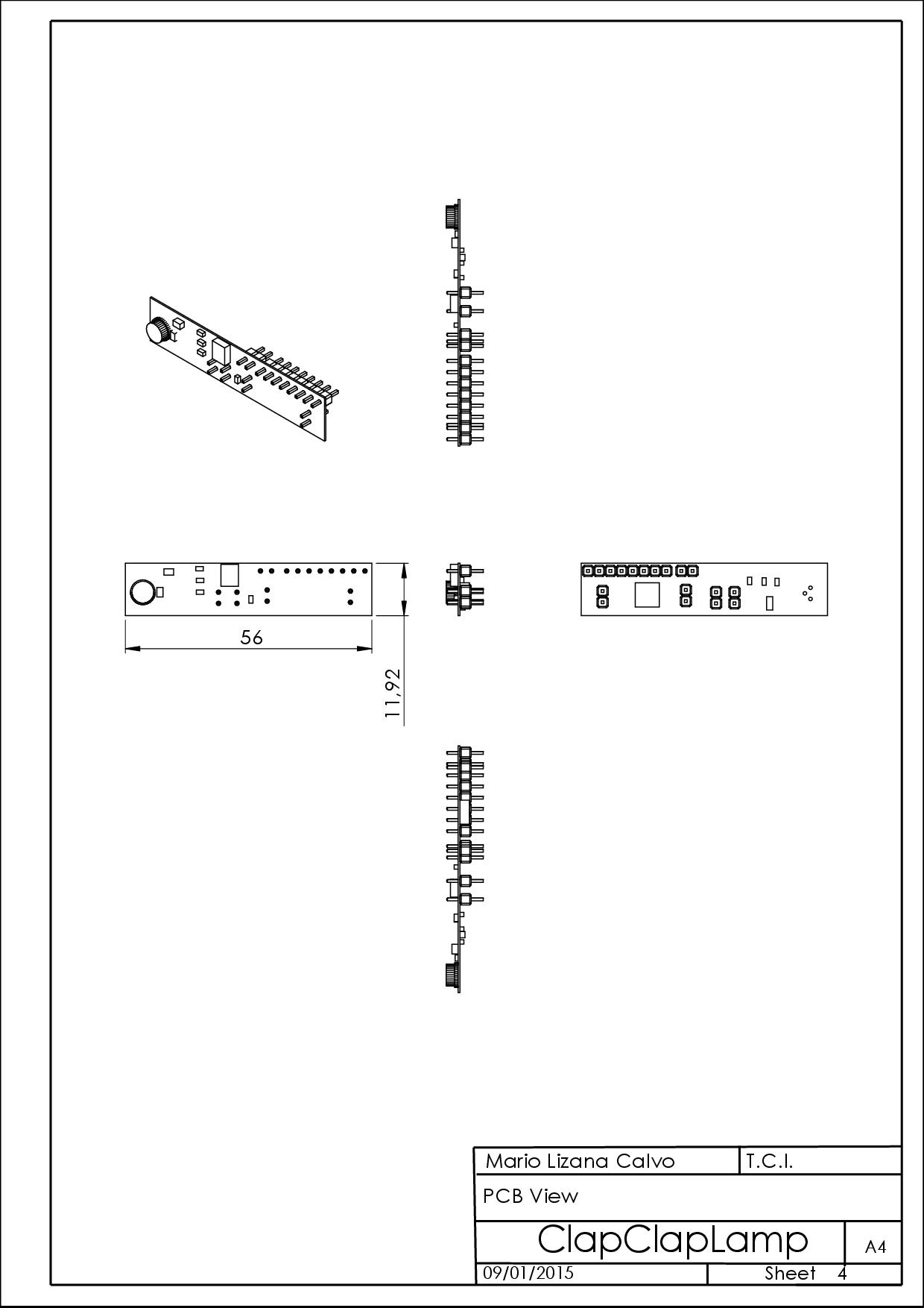
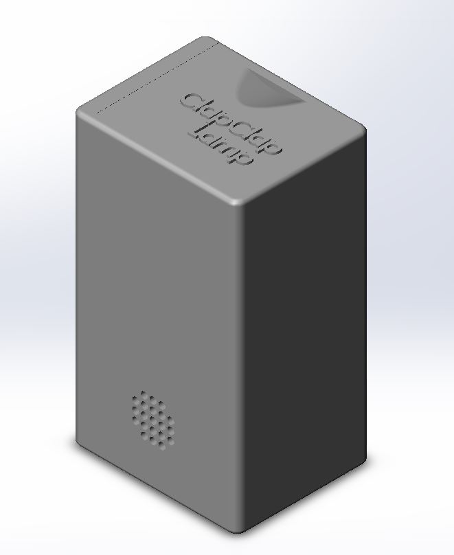
The mechanical design is made in SolidWorks, so it can be easily built with a 3D printer. I am going to show the different parts bounded so it can be reproduced. You can view the images in a bigger size by clicking on it.
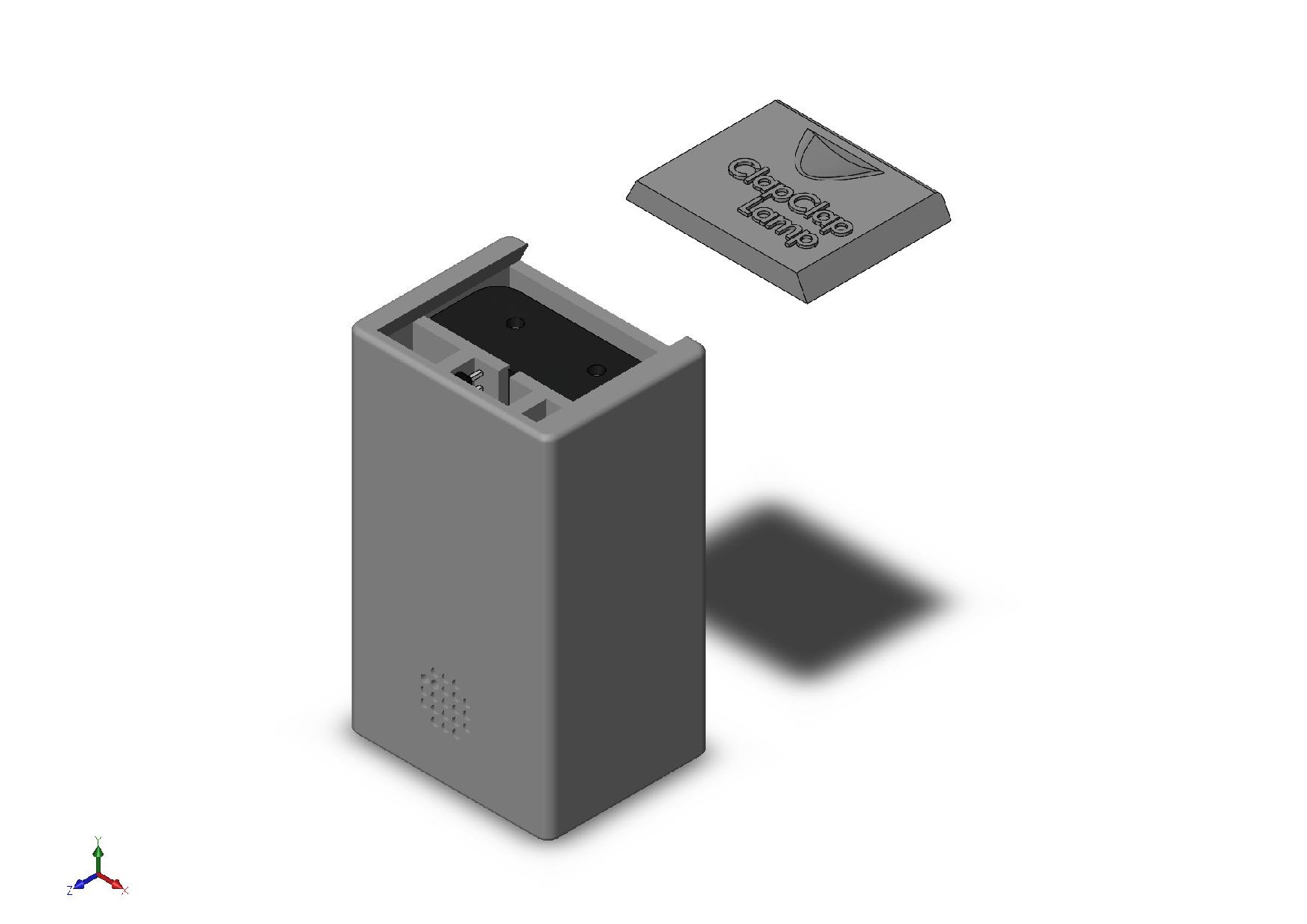
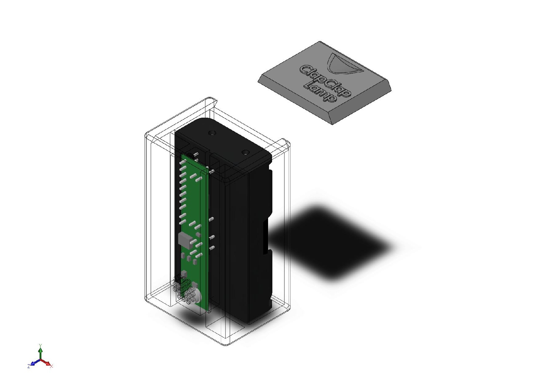
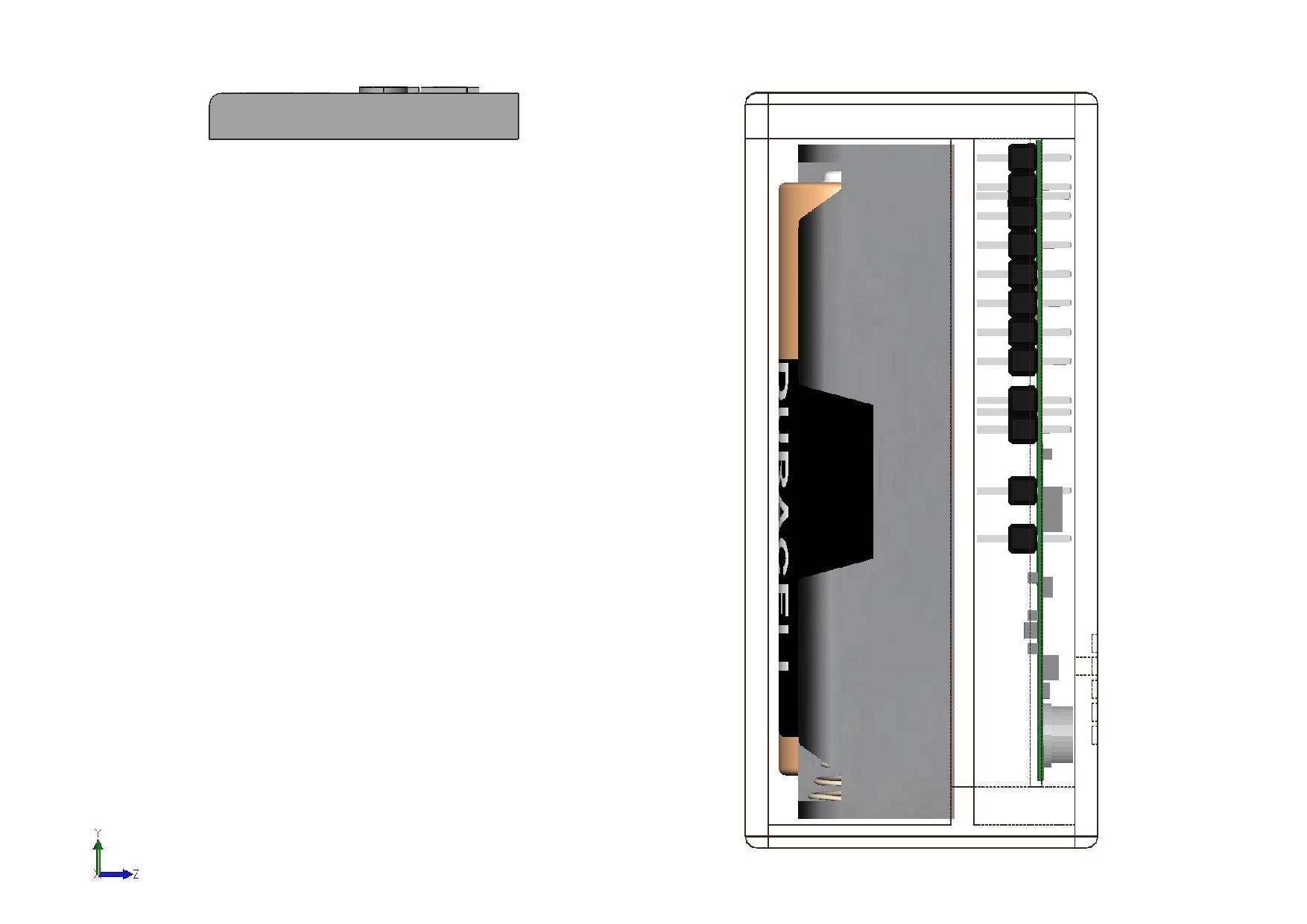
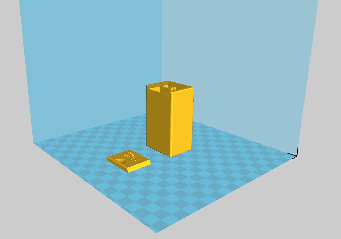
Mechanical Design 1. The whole product.
Mechanical Design 2. Main box.
Mechanical Design 3. Cover.
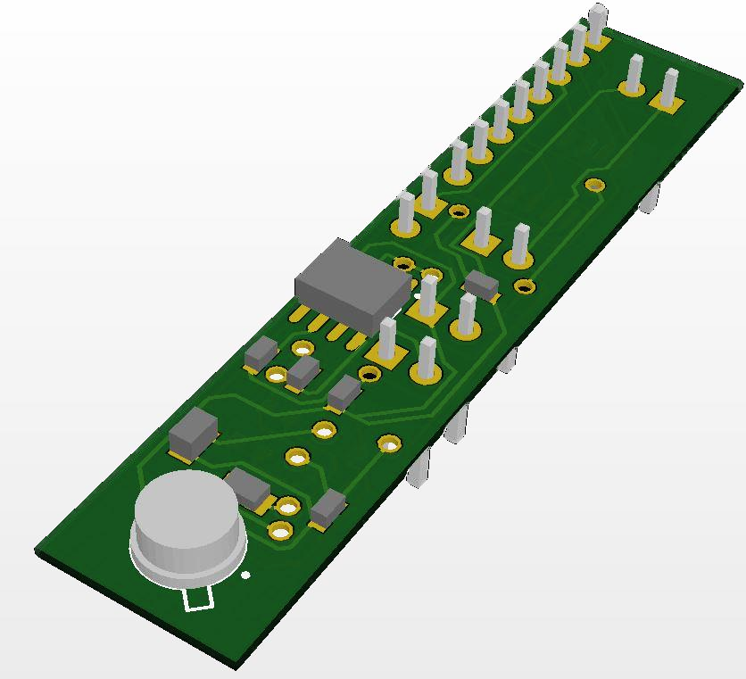
Mechanical Design 4. PCB view.
3D MODEL FOR PRINTING
The box has been designed in SolidWorks which is a user friendly program to sketch whatever object in a computer. Once we have our object finished it's very easy to print it in ABS plastic. We only have to export a .stl file and open it with a 3D printer controller program like Cura Ultimaker. Now you can see some pictures of SolidWorks and the link if you want to download the project.
>Solid Works Project<3D view No. 1.
3D view, No. 2.
3D view, No. 3.
3D view, No. 4.
3D view, No. 5.
3D view, No. 6.
3D view, No. 7.
A external view of the whole product.
3D view, No. 8.
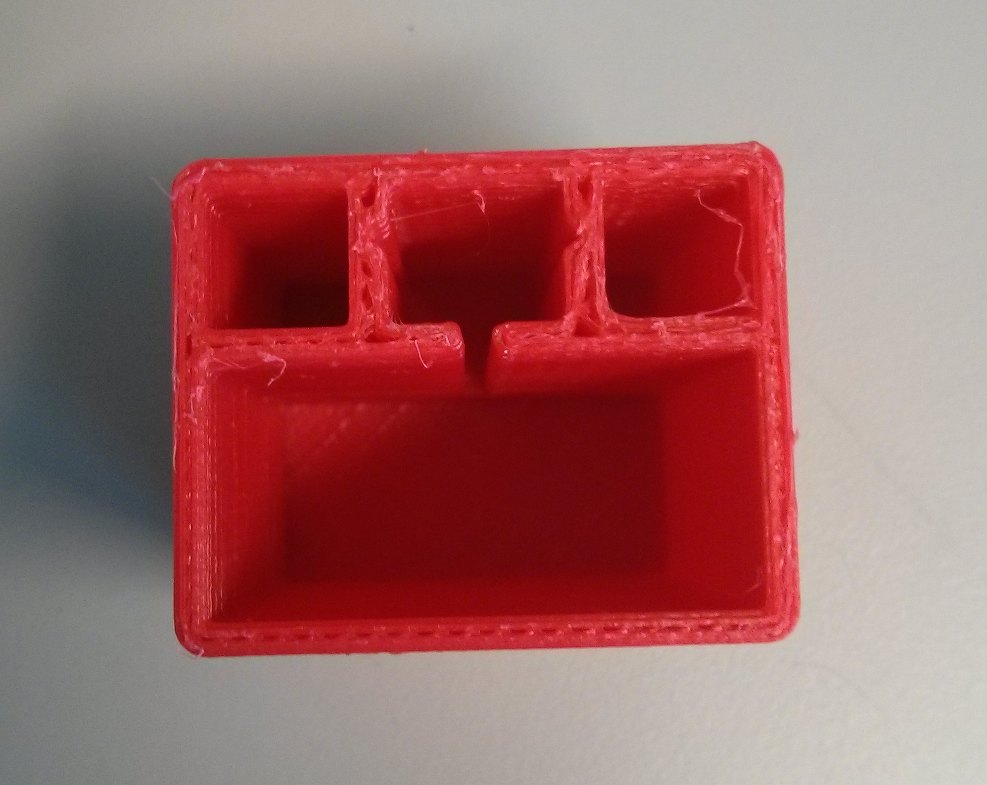
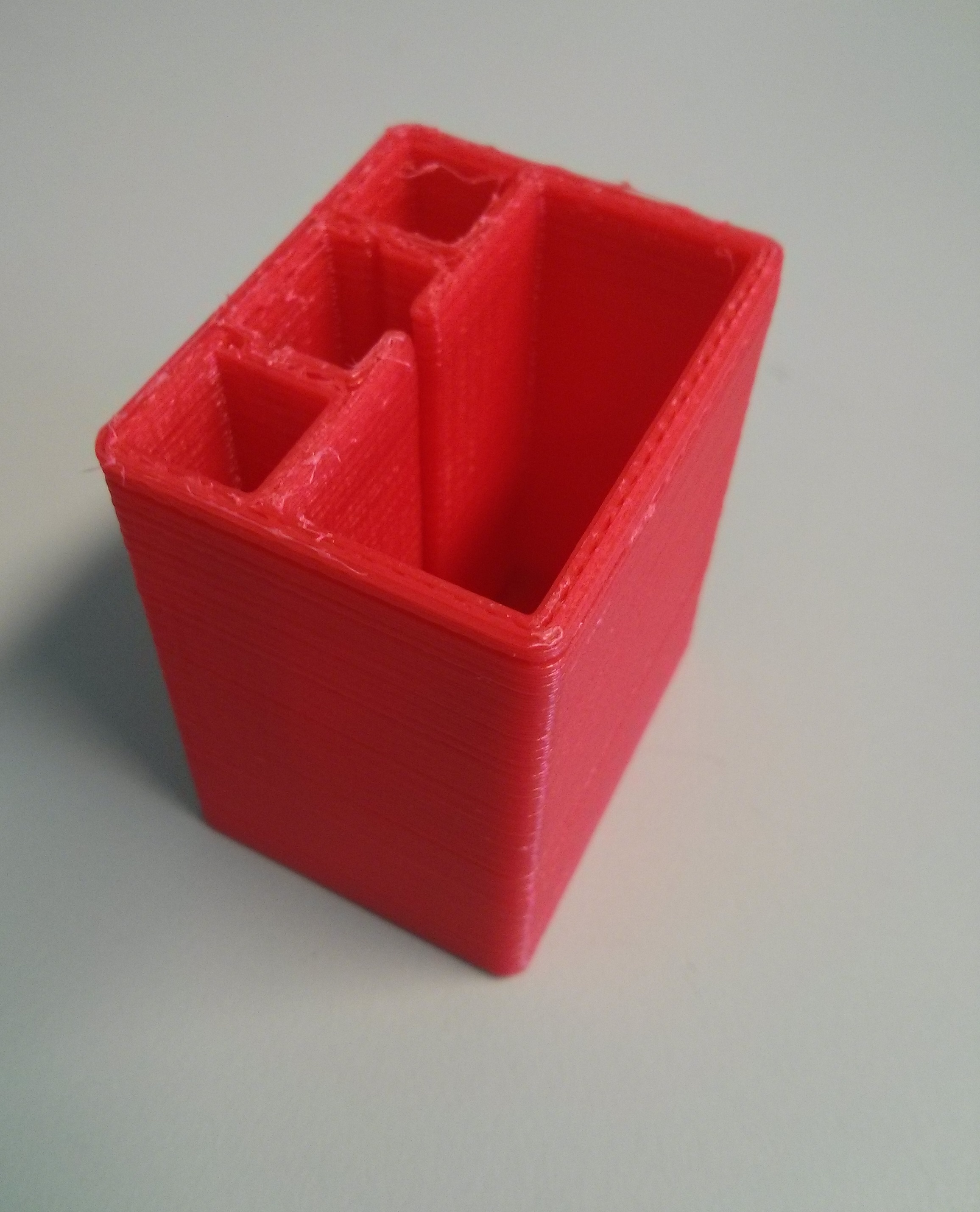
A 3D section of the main box printed in ABS plastic, we can see how is the box inside.
3D view, No. 9.
3D view, No. 10.
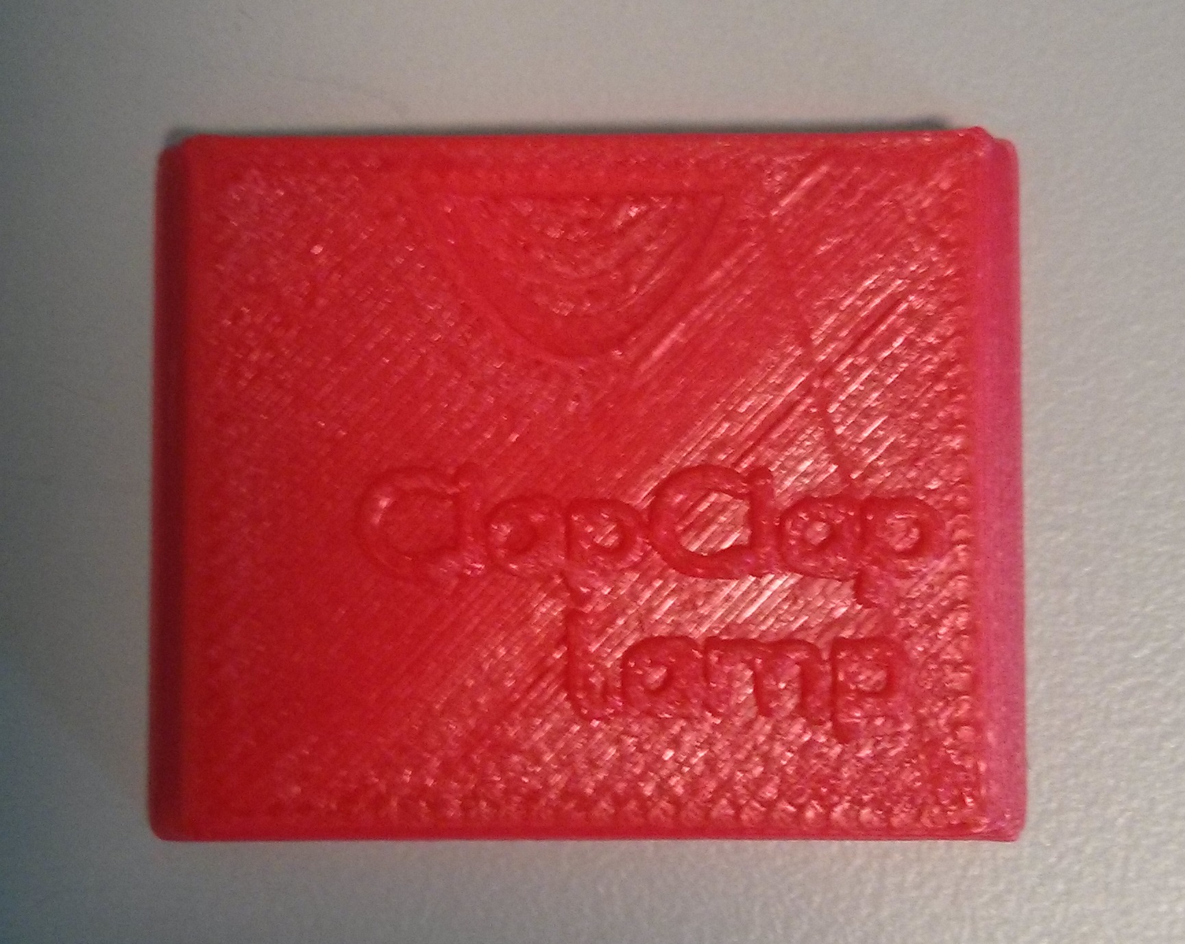
Cover printed in ABS.
3D view, No. 11.
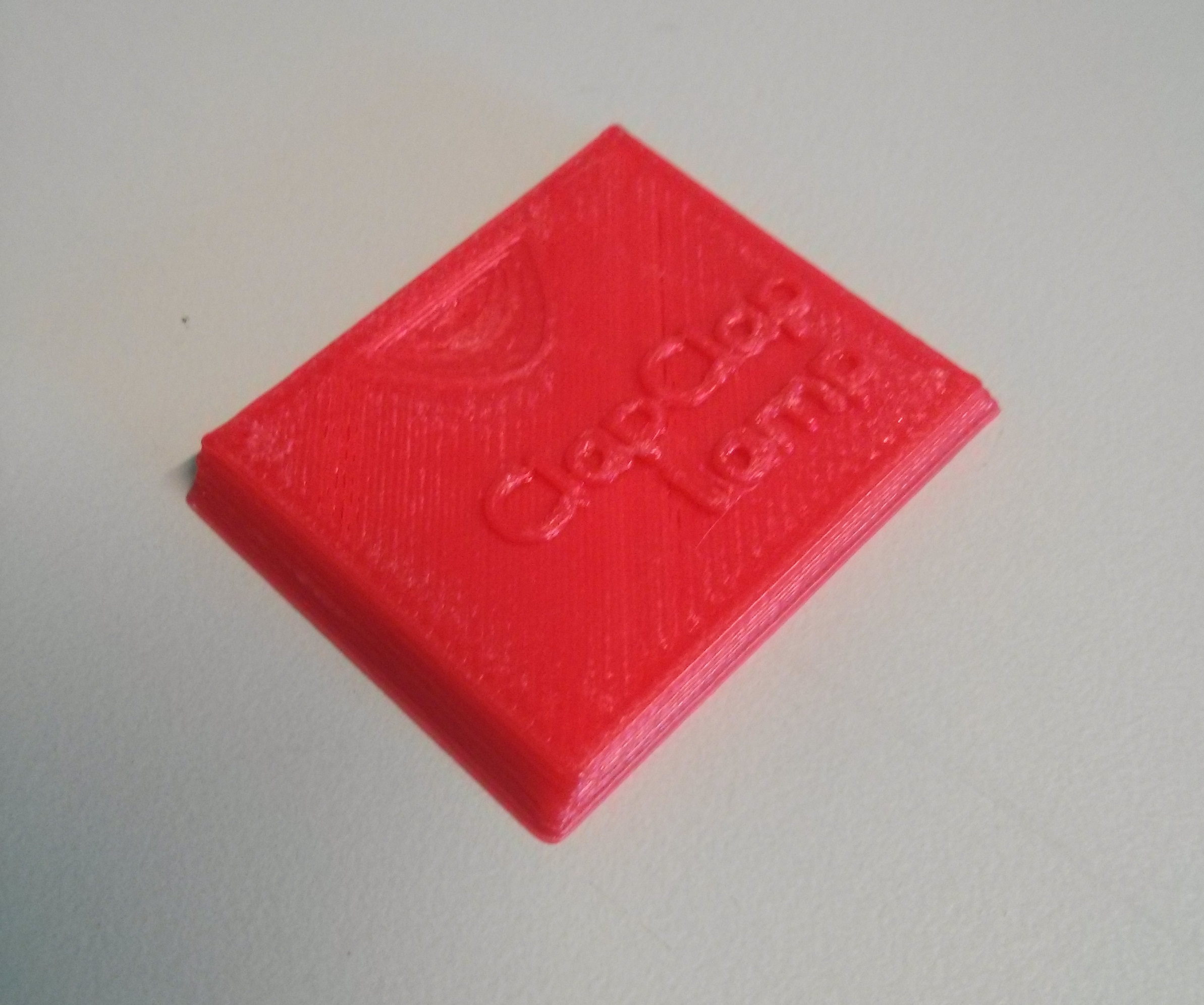
Cover printed in ABS.
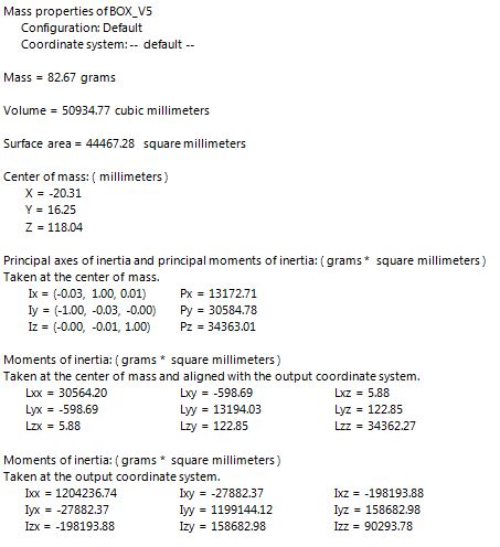
MASS REPORT
We can see my center of mass with the plane of this photo, both of them are coincident, at the other two axis the center of mass is symmetric. The batteries are too heavy compared to the density of the other components, so the center of mass is almost determined by the batteries, even so the center of mass and the center of ClapClapLamp are very closed.
I have made a mass report. The final weight is 82.67 grams, which 51.2 grams are due to batteries. The box of the ClapClapLamp has been simulated as ABS plastic, the batteries have their correct density calculated, the density PCB is determined by Altium and the battery holder is made of ABS PC, which is stronger than ABS. You can download the DOCX file by clicking in the image below.
CURA ULTIMAKER
Let's watch some pictures of the .stl file in Cura Ultimaker.
We can print differents parts of a project at once, as we can see at this picture.
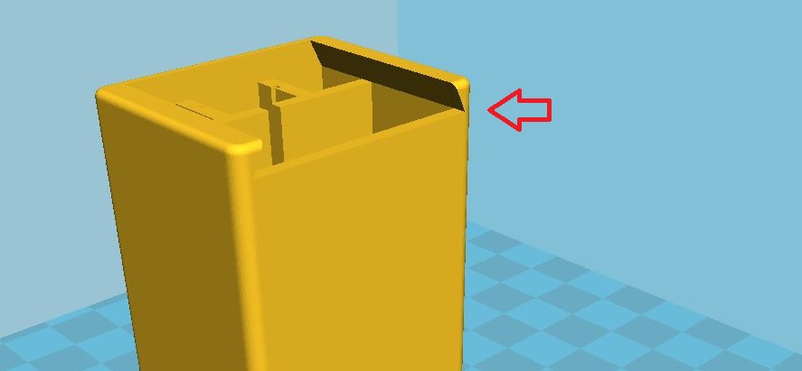
The printing process would have problems if we try to print a horizontal wall, that is why I have not made the cover with a right angle. I'm talking about the angle that is being pointed by the red arrow.
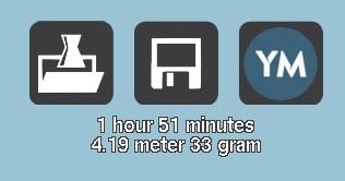
As we can see at the last image, this printing would take 4.19 neters, 33 grams and 1 hour and 51 minutes if we print it with a Prusa I3. Of course, we must configure our 3D printer model in Cura Ultimaker.
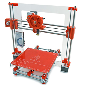
The Prusa I3 Model looks like the photo below, it is a really good 3D printer for it costs.
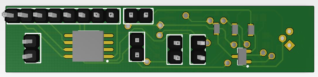
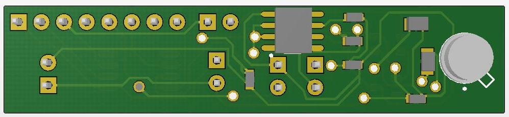
PCB
The PCB has been designed with Altium. I have modified the diameter of the vias, so the PCB can be made with the CNC drilling machine of the lab (0.9 mm). In order to have a realistic 3D model I've had to search in some webpages of 3D models some of the componentes that weren't in Altium. These 3D models are included in the Altium Model.
FIRST SCHEMATIC
Here is the initial prototype of ClapClapLamp. At the beginning I designed it to be supplied with 5V, or even before of 5V I wanted to use a 9V battery, so it has been a challenge to make a design working with 3V.The device is not complex, I have made it with as few components as possible, to make it very cheap.
Here you can download the first schematic project, remember that is not the current schematic (which is further down). >MULTISIM PROJECT<
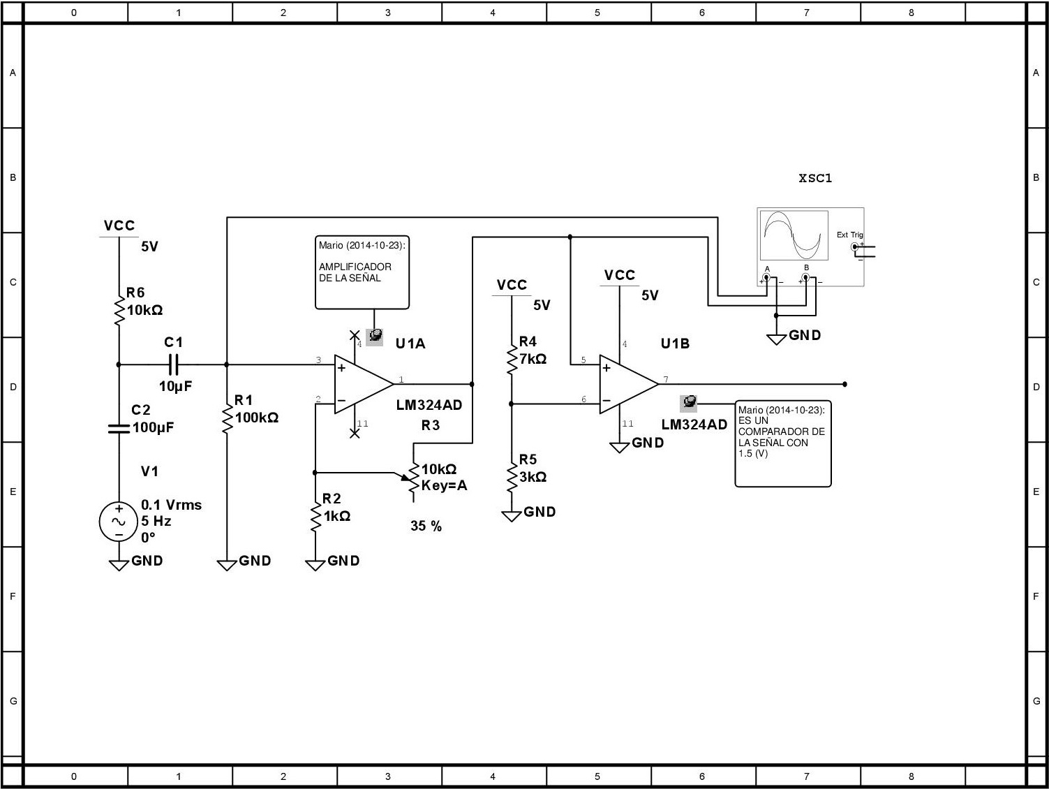
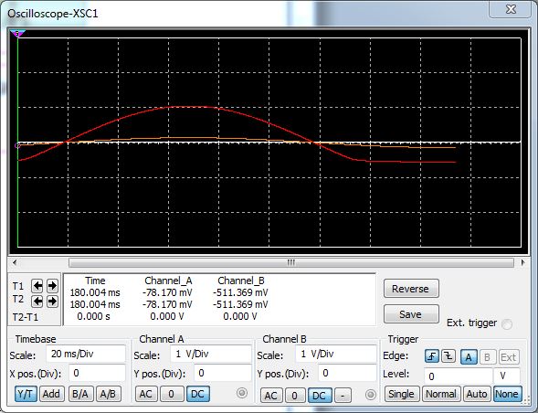
ClapClapLamp has a LM324AD, with two operational amplifiers. One of them is used as an normal amplifier, and the second one like a comparator. In the picture we can see the output of the amplifier, I had an low voltage sinusoidal as input.
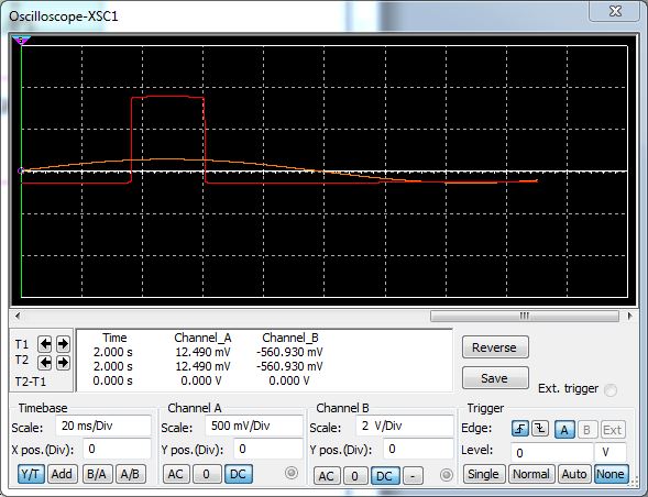
The picture below shows the final output of the circuit, after the comparator. The red signal only get a high level when the low input (acting as the output of the microphone) is at its highest level.
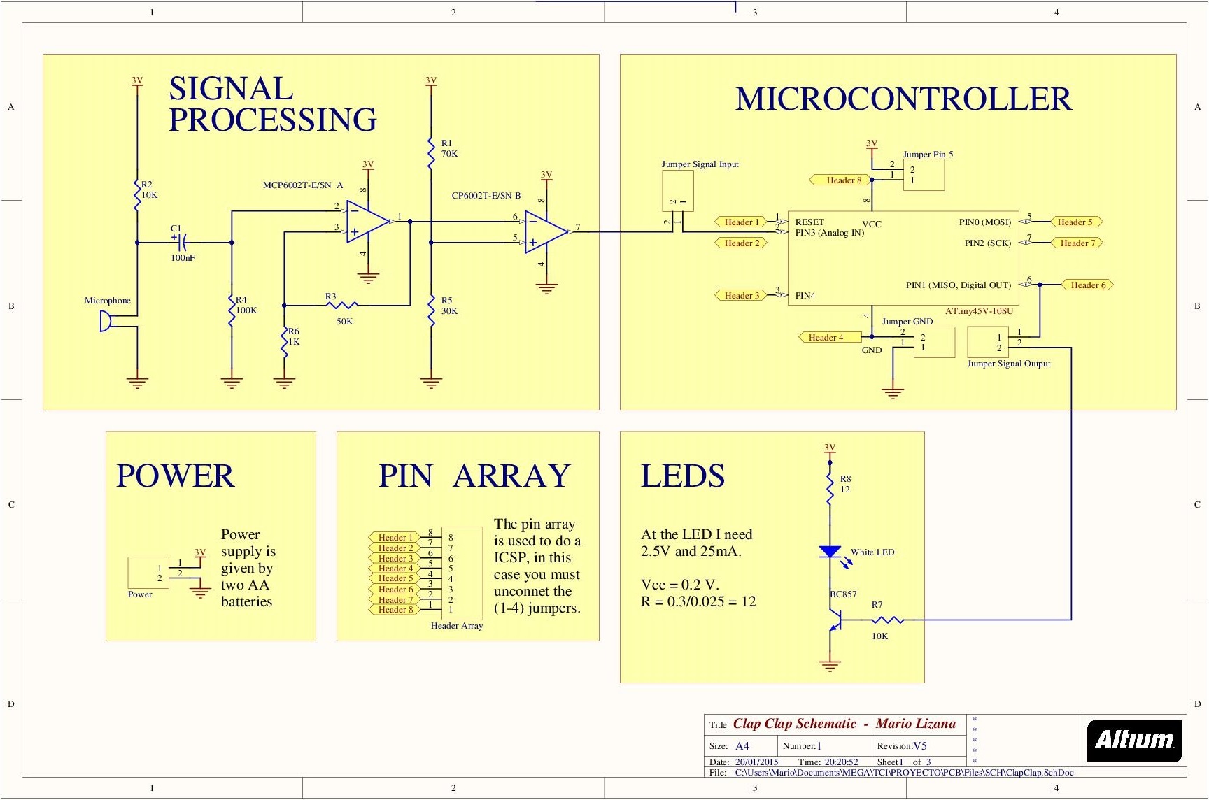
CURRENT SCHEMATIC
The new prototype that I'm using now works at 3V. The schematic has been made in Altium instead of Multisim, and the schematic now has the whole circuit, not only the analog part. I have designed the circuit to be able to program the microcontroller removing four jumpers and connecting a 8 pin header to an external programmer. The 8 pin array is connected directly to the pins of the microcontroller. Altium Project. >LINK<
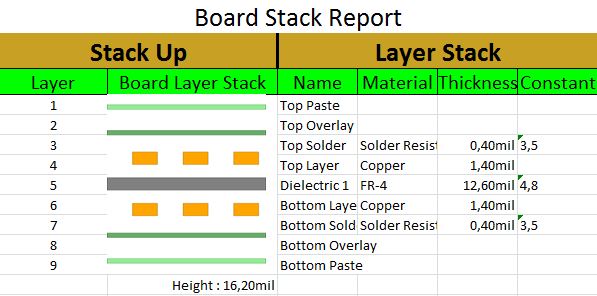
BOARD STACK REPORT
If you click on the image, you'll be able to download an EXCEL file with the board stack configuration used in my design. It is very easy to change the configuration, to make condition it to your lab.
BOARD SPECIFICATIONS
WHOLE BOARD INFORMATION REPORT
Here you can get a whole information about all the configurations taken to design the PCB.
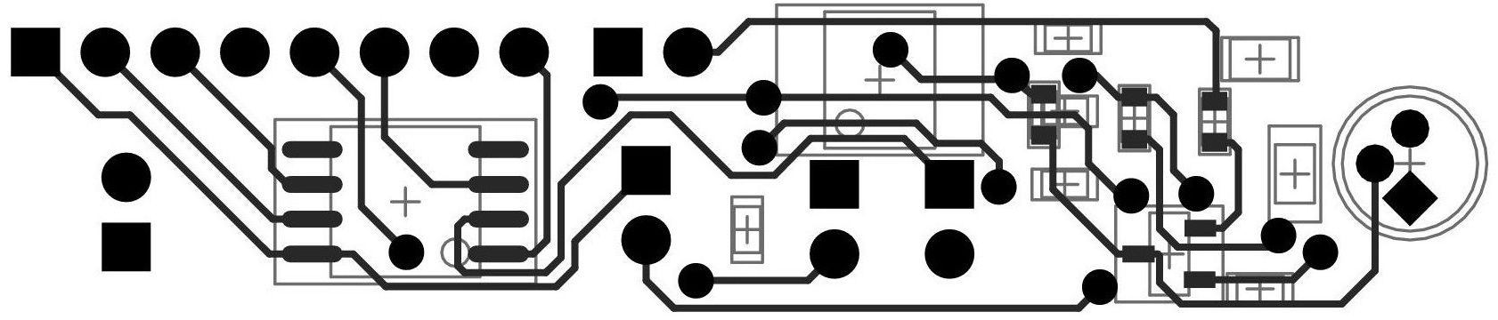
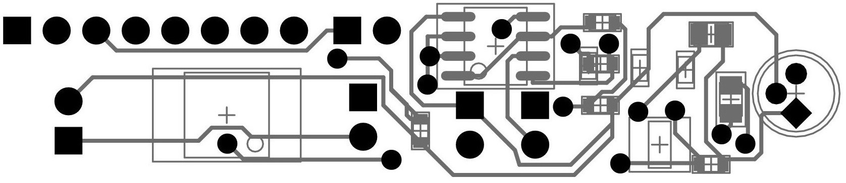
>BOARD SIMULATION REPORT<PCB TRACKS
At this images we can see a "map" of the project tracks, these are required for the PCB fabrication. I'm going to show the two most important images generated for the fabrication where we can watch the tracks generated. Altium make a lot of files that are important to the fabrication process, like solder paste stencils, the printable label of the componentes, etc.
It has been difficult to route all the tracks due to the lack of space and to the through hole connectors. I could have made a larger PCB, but I challenged myself to reduce the area as much as possible.
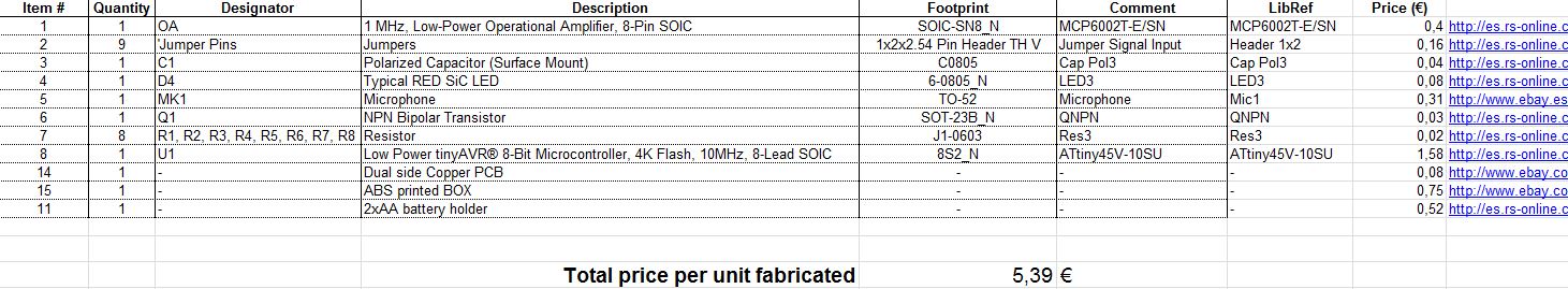
BOM
The bill of materials is given below. You can download an EXCEL and get the links of each component by clicking at the picture. All components have been searched in RS or EBAY.

DESOLDERING SMD
At the first video you can see the first time ever I tried to desolder a SMD component.
In my defence, I have learnt a bit about desoldering from that day. Seeing it now I think that I did not have enough heat at the solder equipment yet.
At this try I was be able to desolder some SMD componentes :)
Now let see some componentes I desoldered with the hot air gun. There are some through hole components, I desoldered them with the vacuum desoldering gun. Unfortunately I only took two photos one day.
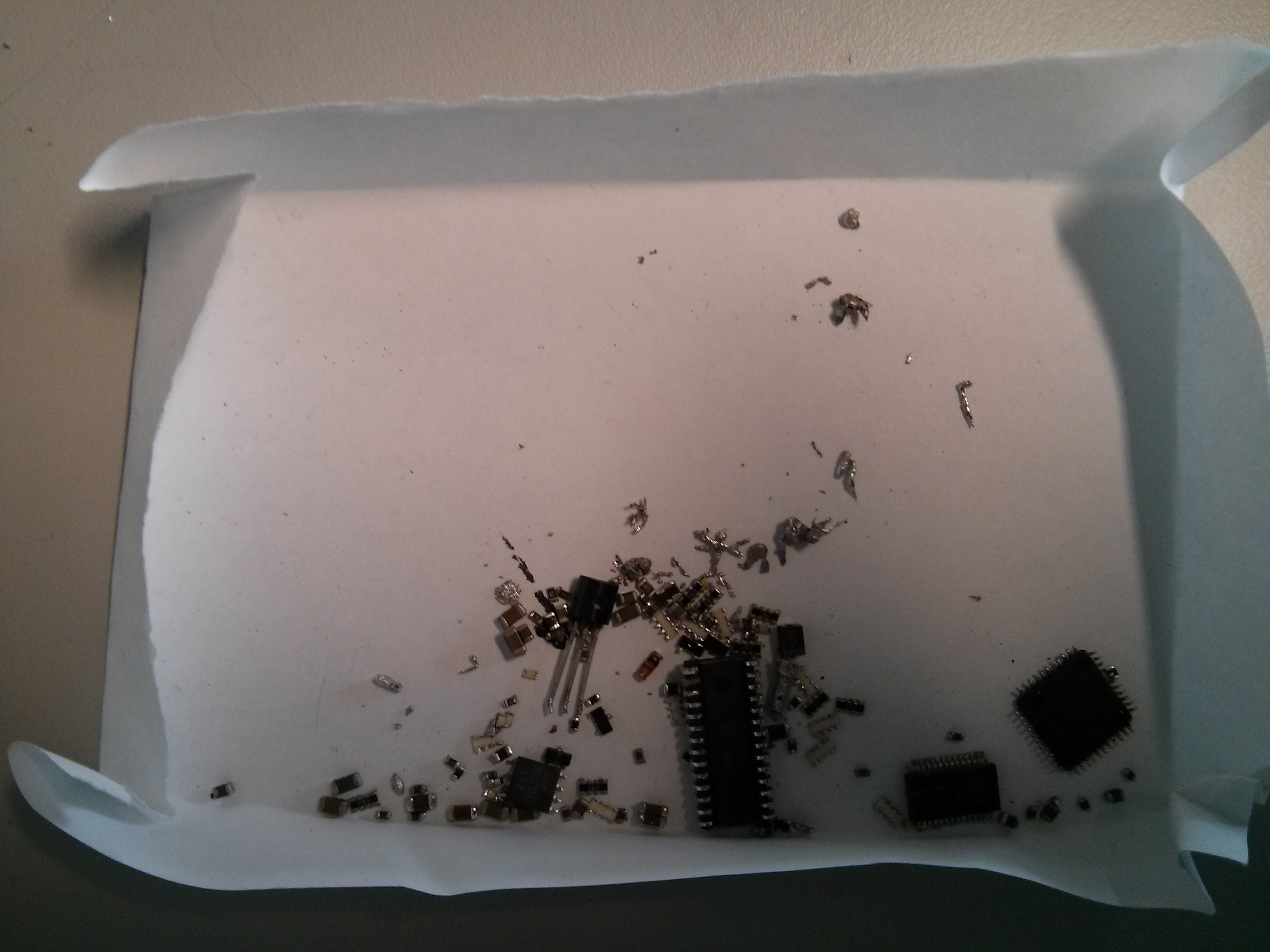
Here is the other photograph; it's a relay. I remember I also took out some connectors and the quartz oscillator.
COPPERCLAD PROJECT
INTRODUCTION
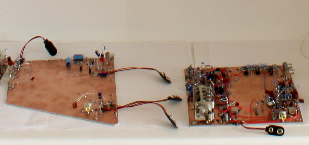
Copper clad is a technique for rapid prototyping of circuits, widely used in RF. This photo shows a RF circuit made on a copper clad. I have been part of a project to make an electric piano, not exactly in copper clad, we wanted to make it supported by copper wires. The project is not finished although most of the circuit are already and tested (like my circuit), ready to be assembled.
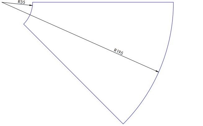
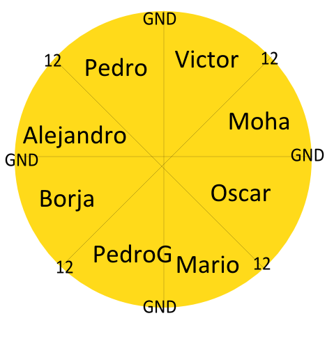
DIMENSIONS
The platform is divided by 8 parts, one for each component of the project. The images further down shows the dimensions of each part (made by Victor Burgos Gonzalez). The final product is designed to be circular. The circuits are activated by a hand shadow, controlled with the reset input of the 555 integrate and a LDR resistor.
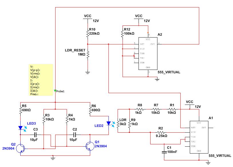
MY CIRCUIT
Each section is supposed to make a different frequency sound, my frequency is 329.63 Hz. I did not want to make just an oscillator, so I introduced two leds. These leds are controlled by a flip-flop circuit. The oscillator have it frequency determined by a variable resistance and another resistance of 22K Ohm (I have design this 22K resistor to be some resistors in series) . One of the leds of the flipflops is glued to a LDR which is in parallel to one of the resistor used to make the 22K resistor. It's hard to explain, It is better to see the circuit. You can download the simulation of my circuit at the following link.>SIMULATION<
I wanted to have a low frequency sound appart from the 329.63 Hz one. And it works! Here you can find a photo of my prototype and a video.
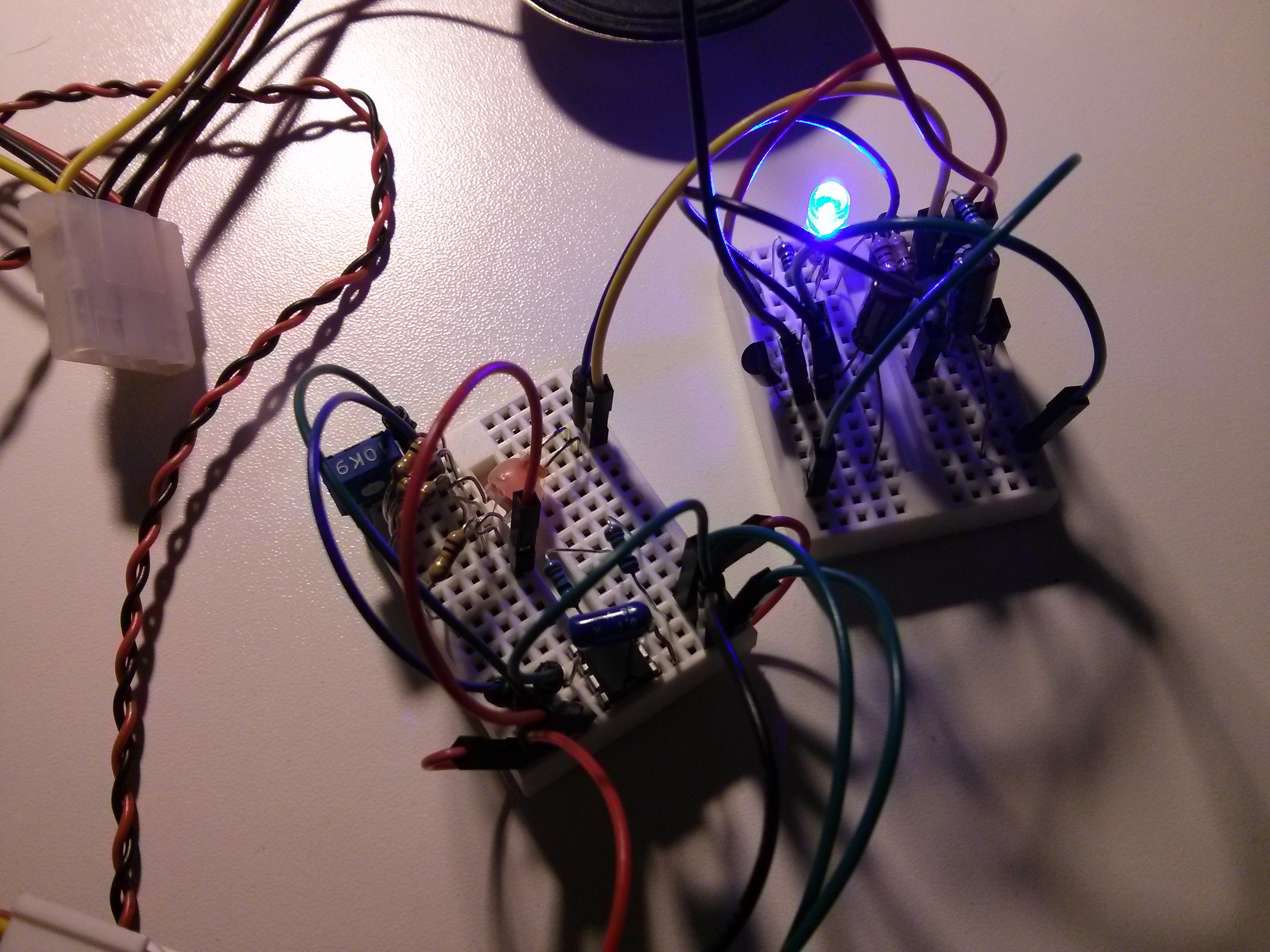
I think it sounds great! :)
FUSES WITH PCB TRACKS PROJECT
INTRODUCTION
You know how a fuse works, right? The fuse has a very thin filament which get very hot when a current pass through it. When there are more current than the allowed the filament reaches the fusing temperature and breaks.
DESIGNING OF FUSES IN A PCB
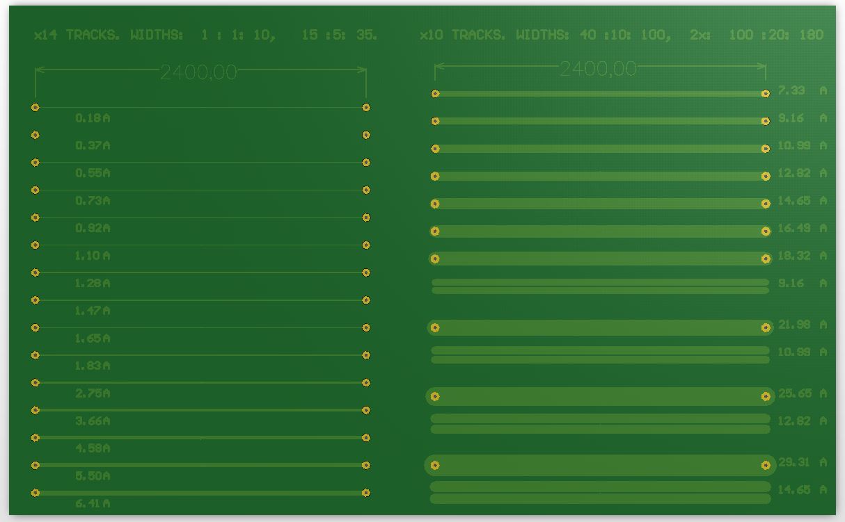
We can make it also with PCB tracks, at this project I have designed a PCB board with a lot of tracks, each one with a different width, so each one can allow a different current before it breaks. The maximum current has been calculated with the Onderdonk formula, which calculates how many amps we need for fusing a track of "X" mils of width in "Y" seconds. The width and the time can been changed In a .ODS file for recalculate the new ampere value.
>.ODS FILE FOR CURRENT CALCULATION<At the image below you can see a 3D simulation of the PCB in Altium. The tracks has their dimensions and the needed amperes for being broken in two seconds. I have used two tracks for the tracks with a width higher than 100 mm, a normal one and the other divided by two. In order to check if the fuses have the same behaviour.
Here you can download the Altium project in case you want to use it. >ALTIUM FILE <
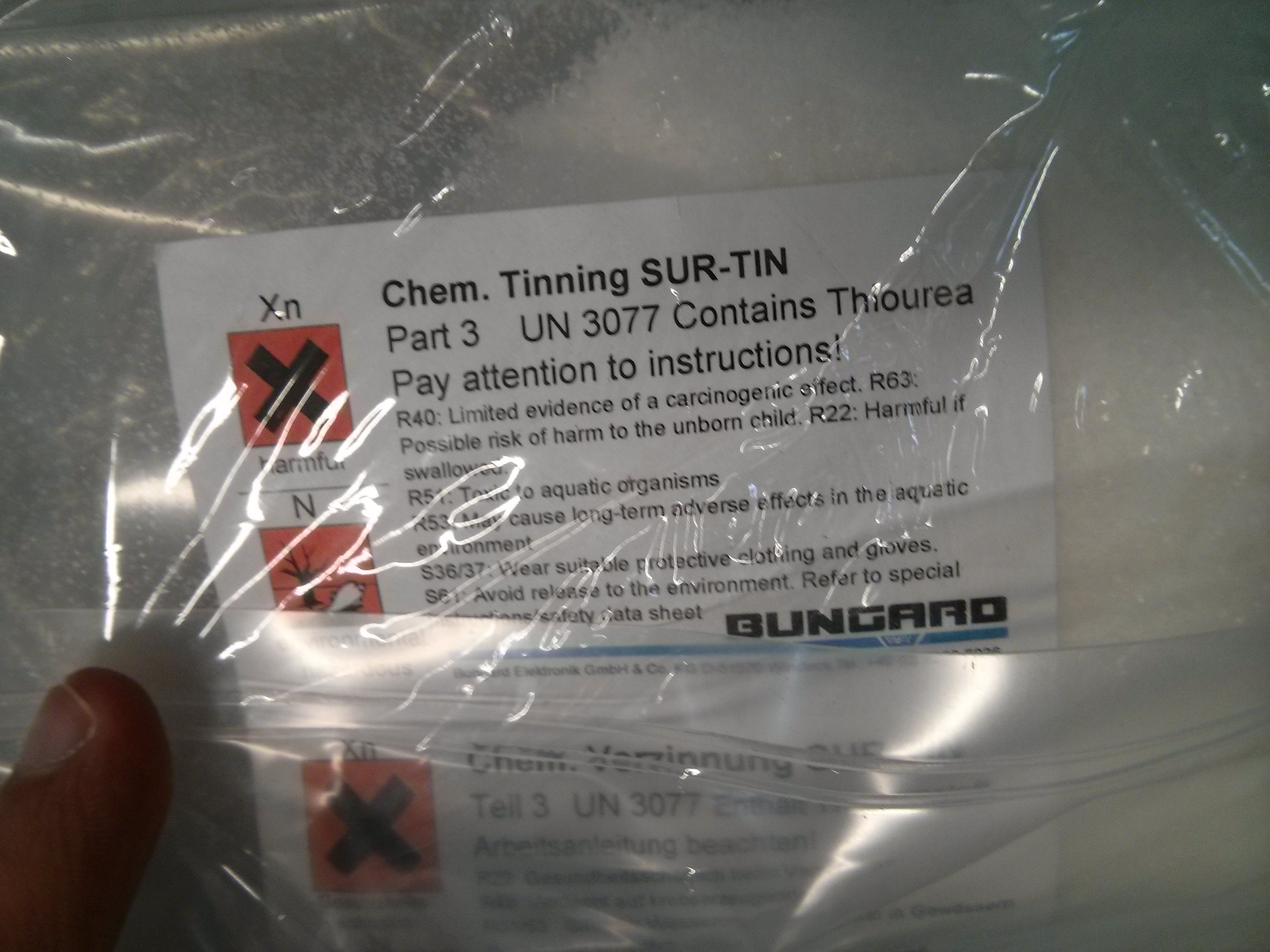
ELECTROLESS TIN PLATING PROJECT
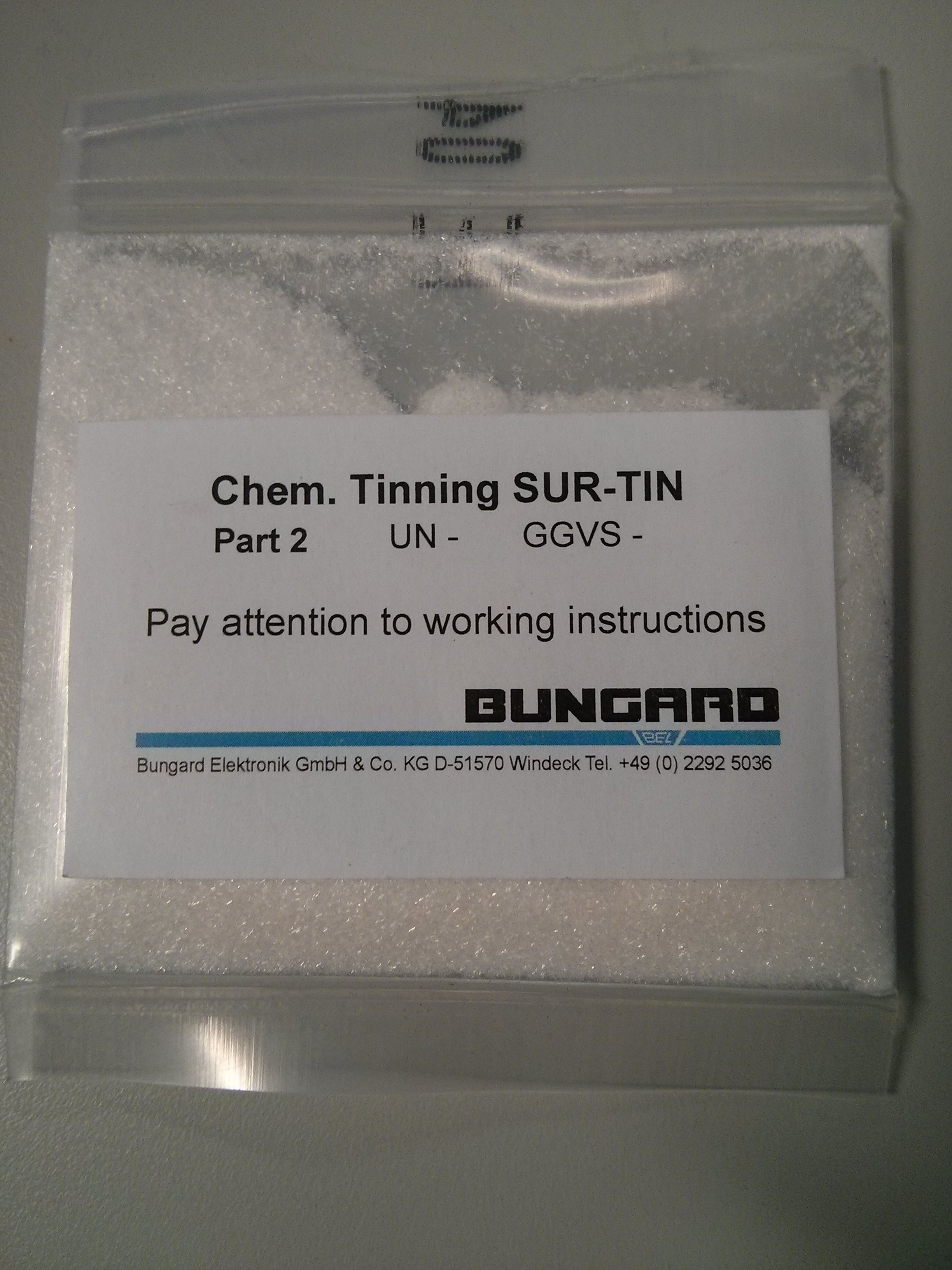
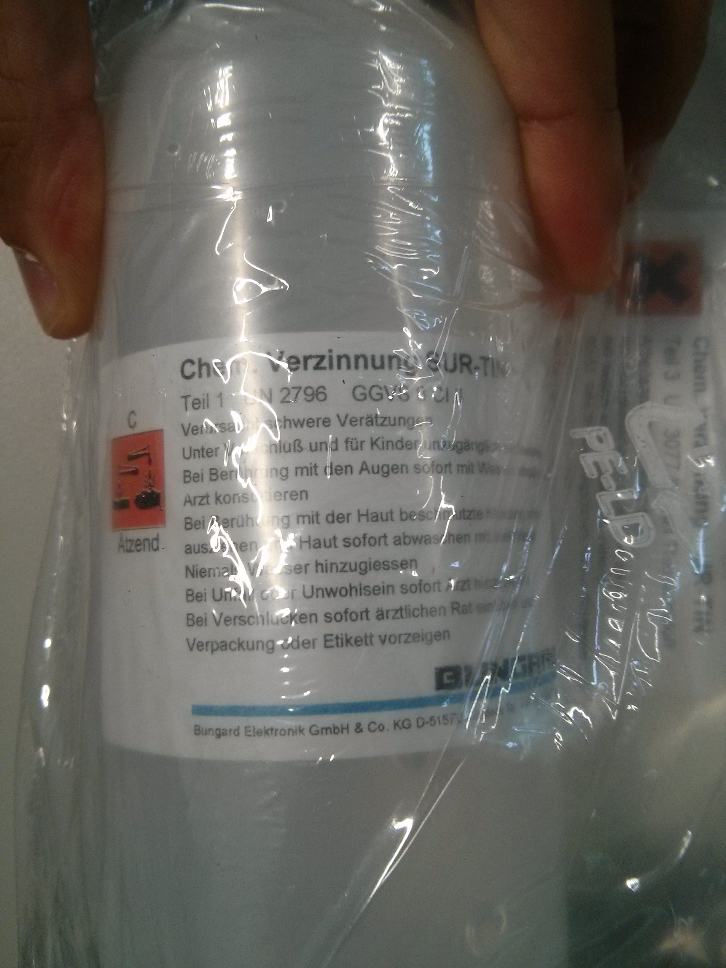
In the lab we have tin plating products so we can make tin plating to protect the copper of the PCB we have made. My target was to find some intruction to make the tin plating.
Some photos of the product available atthe lab.
I found some videos in youtube making electroless tin plating. It's very simple, as you can see in the youtube video below.
>Youtube Link< Despite of having found videos like like the one above, I continued searching in case I would find a manual with the same brand and model of the lab product, and I found this PDF of C.E.G, an official partner of the product brand in Spain. The instructions are well explained. Here yo have the PDF.
>Electroless tin plating instruction.<
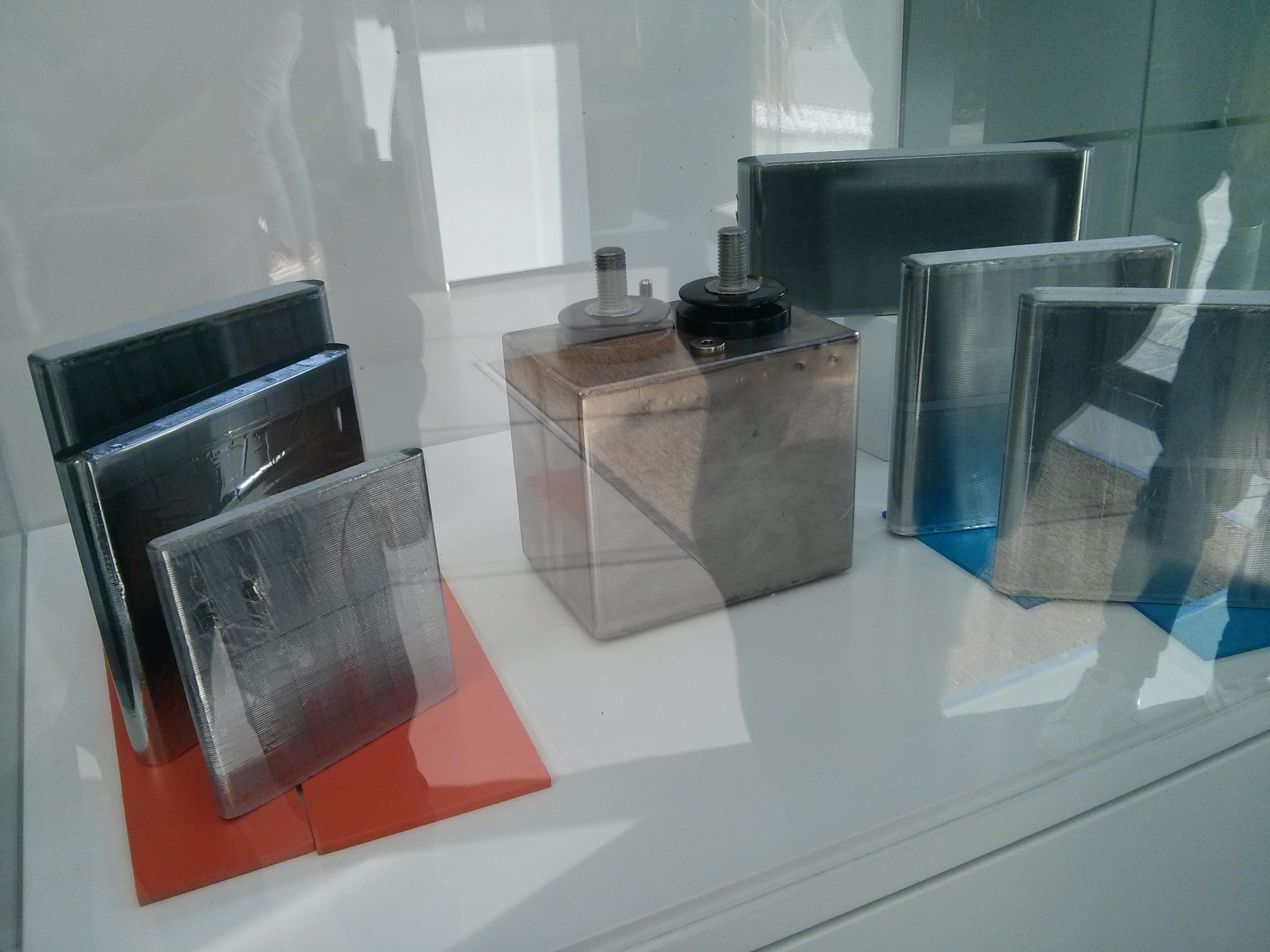
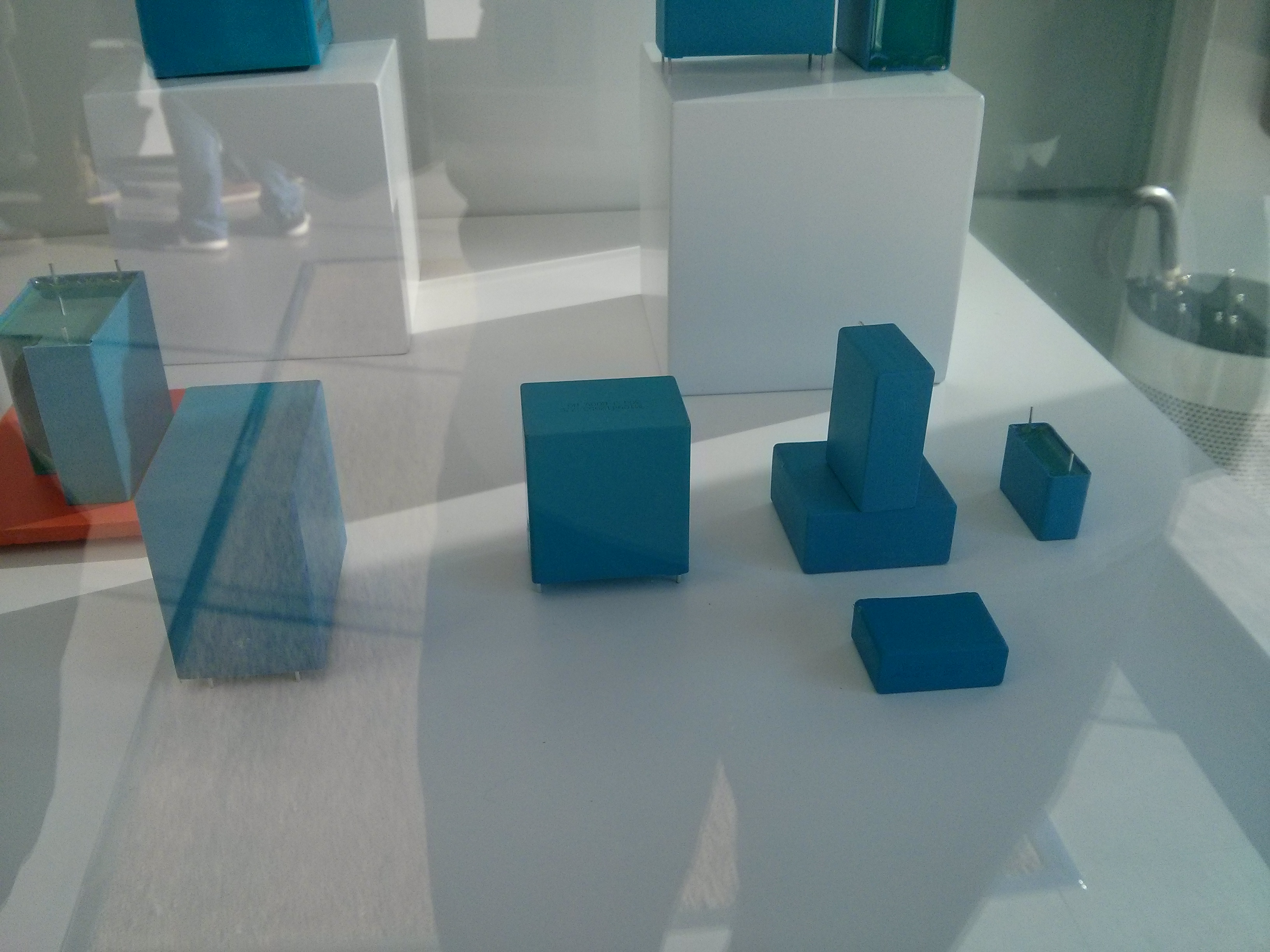
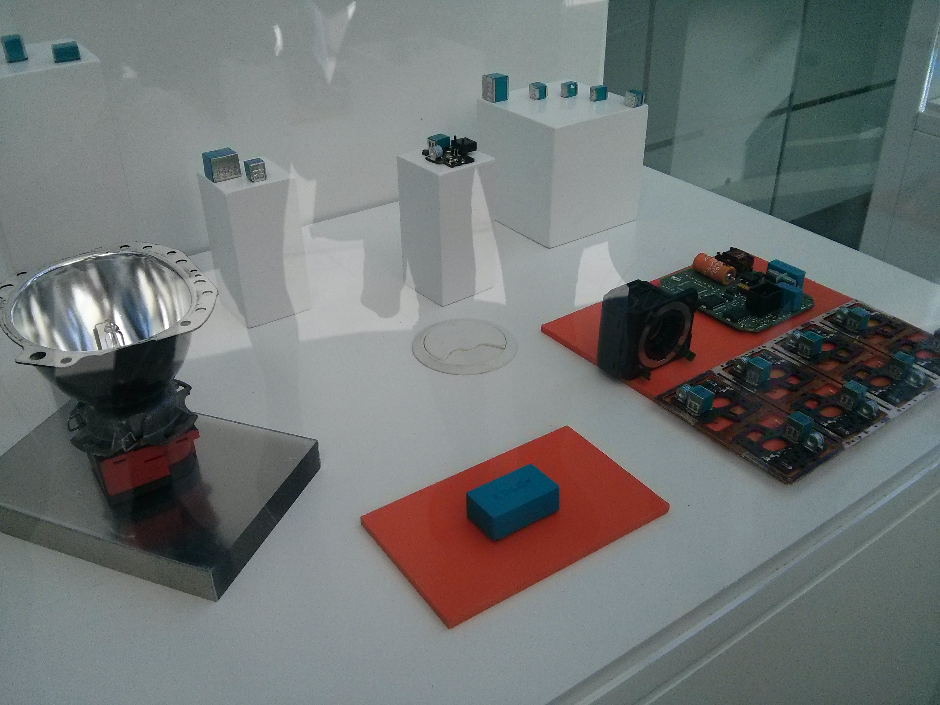
FIELDWORK
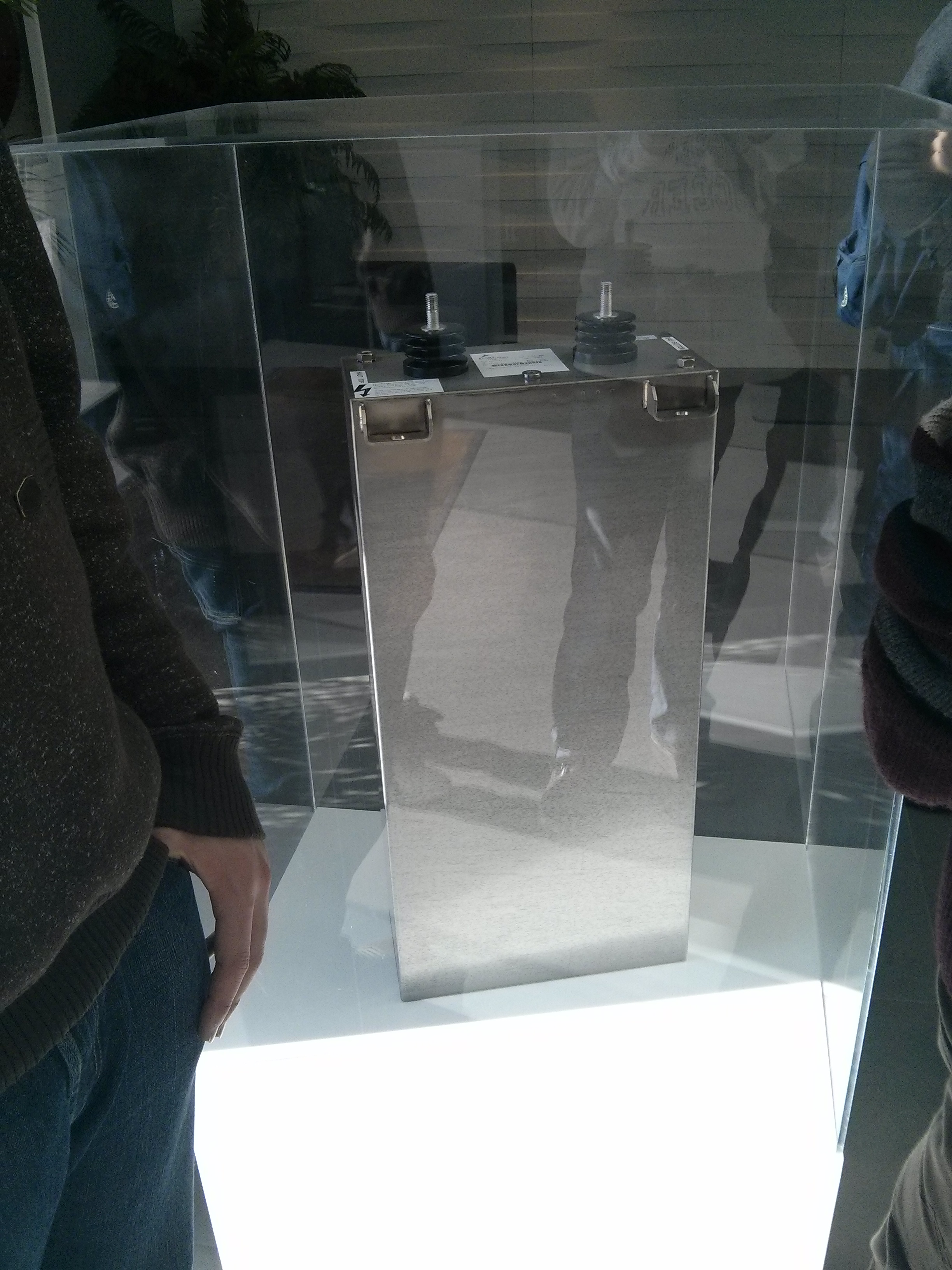
Some photos of our fieldwork. It is a pity I only took photos in one of the companies; TDK. Everything you see in the pictures are capacitors.

CONCLUSION AND PERSONAL EVALUATION
I only know I don't know anything, it's my feeling about the TCI course, and also about my way in university. There are so much thing I would like to learn that I don't know what to do first!
With this course I have learnt a lot about programs currently been used in electronic engineering. May be the only disadvantage I would say about TCI is the lack of time, a lot of things to learn and all of them interestings.
Relating to my project, I would like to have had more time in order to make the PCB and to see it working.